Phase change memory

A phase-change memory and memory technology, applied in the field of memory and phase-change memory, can solve the problems of wasting the writing speed of phase-change memory, limiting the scope of use, etc., so as to improve the overall writing speed, increase the writing speed, and accelerate the bus frequency. Effect

Active Publication Date: 2012-07-04
SHANGHAI INST OF MICROSYSTEM & INFORMATION TECH CHINESE ACAD OF SCI
View PDF2 Cites 0 Cited by
  • Summary
  • Abstract
  • Description
  • Claims
  • Application Information

AI Technical Summary

Problems solved by technology

However, this method requires strict requirements on the addresses of the two data writes before and after, which limits its scope of use.
[0006] Since the time required for RESET and SET is different, and the SET time is longer than the RESET time, so in the phase change memory parallel writing process, the writing time of each byte is determined by the SET time, while the bit for the RESET operation is in the wait state, thus wasting the write speed of the phase change memory

Method used


Image

  • Phase change memory
  • Phase change memory
  • Phase change memory

Examples


Embodiment 1

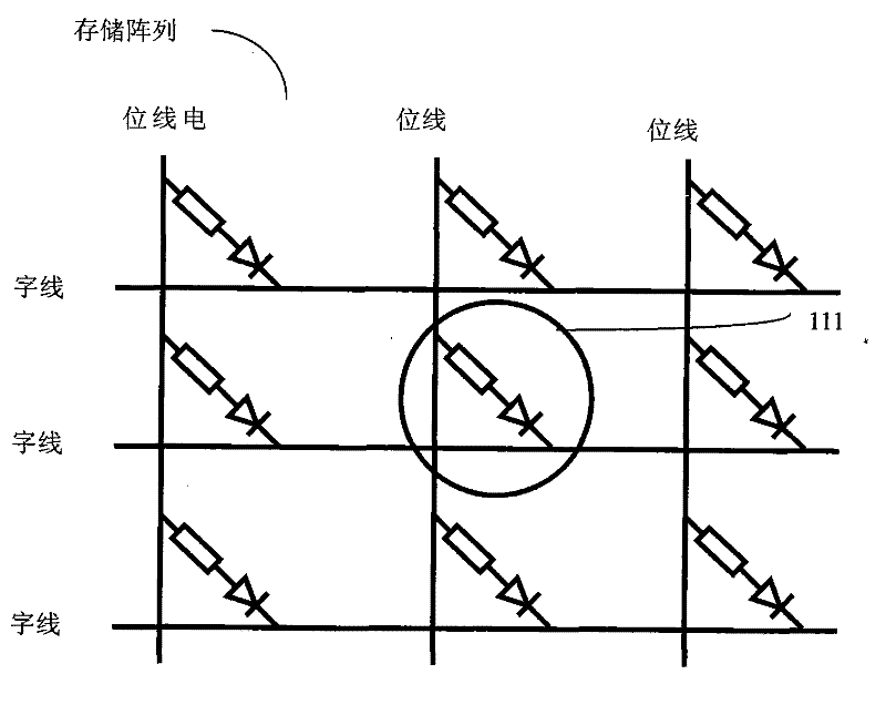
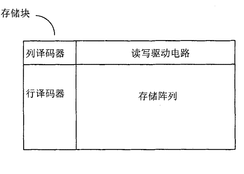
[0038] The invention discloses a phase-change memory, which includes several storage wing planes; the plane includes n storage blocks and n first-in-first-out stack FIFOs, each block corresponds to a FIFO; wherein, n It is a phase change memory to read and write bits in parallel; planes are connected by data bus, address bus and control bus; the data bus transmits write data or read data, the address bus transmits addresses, and the control bus transmits read and write signals. The block includes a storage array, a row and column decoder and a driving circuit. Inside the plane, the FIFO receives read and write signals from the bus.

[0039]When the write signal arrives, the FIFO downloads the data and address to be written from the bus; each FIFO unit stores both the information of the currently written data and the address information of the currently written data; or the FIFO unit only stores the Information about the currently written data. Blocks are written according to...

Embodiment 2

[0071] The present invention proposes a method capable of accelerating the overall burst write speed for the burst write mode of the phase change memory. The so-called burst write method means that a large amount of external data needs to be stored in the memory. In this way, generally, the external bus controller transmits the data to be written to the external bus at a certain frequency, and the memory receives a write command from the external bus, writes data and addresses, and performs a write operation. Due to the huge amount of data, in this method, the speed of writing data alone is usually not considered, but the speed of writing data as a whole is considered, and parallel writing is usually used for multi-bit writing.

[0072] The present invention adopts the following structure to improve the overall writing speed:

[0073] The phase change memory is composed of several storage planes, and each plane is composed of n storage blocks (block) and n first-in-first-out ...


PUM


Abstract

The invention discloses a phase change memory, which comprises a plurality of memory planes, wherein each plane comprises n memory blocks and a first in first out stack (FIFO); each block corresponds to one FIFO; n is a concurrent read and concurrent write bit number of the phase change memory; the planes are connected through a data bus, an address bus and a control bus; and the block comprises a memory array, a row and column decoder and a drive circuit. The phase change memory provided by the invention has improved writing speed; and each bit independently acquires data from the FIFOs so as not to be influenced by the SET operation of the other bits, like a conventional concurrent writing mode, when a RESET or SET operation is performed on the bit, and waiting time after the RESET operation is further shortened.

Description

technical field [0001] The invention belongs to the technical field of micro-nano electronics and relates to a memory, in particular to a phase-change memory capable of improving the writing speed of the phase-change memory. Background technique [0002] Phase change memory technology is based on Ovshinsky's proposal in the late 1960s (Phys. Rev. Lett., 21, 1450-1453, 1968) and early 1970s (Appl. Phys. Lett., 18, 254-257, 1971) The idea that the phase change film can be applied to the phase change storage medium is established, and it is a storage device with low price and stable performance. Phase-change memory can be made on a silicon wafer substrate, and its key materials are recordable phase-change films, heating electrode materials, heat-insulating materials, and lead-out electrode materials. Including how to reduce device material and so on. The basic principle of phase change memory is to use electric pulse signal to act on the device unit, so that the phase change ...

Claims


Application Information

Patent Timeline
Patent Type & Authority Patents(China)
IPC IPC(8): G11C11/56
Inventor 丁晟宋志棠
Owner SHANGHAI INST OF MICROSYSTEM & INFORMATION TECH CHINESE ACAD OF SCI
Why Eureka
Try Eureka