Element layout capable of increasing layout efficiency and integration degree

A technology of integration and devices, applied in the field of device layout, can solve the problems of reducing layout efficiency, increasing layout design complexity, reducing device integration, etc., to achieve the goal of improving layout efficiency, reducing distance, and increasing integration Effect

Inactive Publication Date: 2010-07-28
SHANGHAI HUAHONG GRACE SEMICON MFG CORP
View PDF4 Cites 7 Cited by
  • Summary
  • Abstract
  • Description
  • Claims
  • Application Information

AI Technical Summary

Problems solved by technology

[0004] The above-mentioned insulation isolation between LDMOS and other components by separating a certain distance has the following problems: First, it is necessary to define design rules for the isolation distance. When the drain voltages of LDMOS are different, it is necessary to target Different isolation distances in voltage design increase the complexity of layout design and reduce layout efficiency; moreover, all LDMOS and LDMOS and other components are separated by a large distance to achieve insulation isolation, which will reduce the integration of devices. Spend

Method used


Image

  • Element layout capable of increasing layout efficiency and integration degree
  • Element layout capable of increasing layout efficiency and integration degree
  • Element layout capable of increasing layout efficiency and integration degree

Examples


Embodiment Construction

[0016] The device layout that can improve the layout efficiency and integration of the present invention will be further described in detail below.

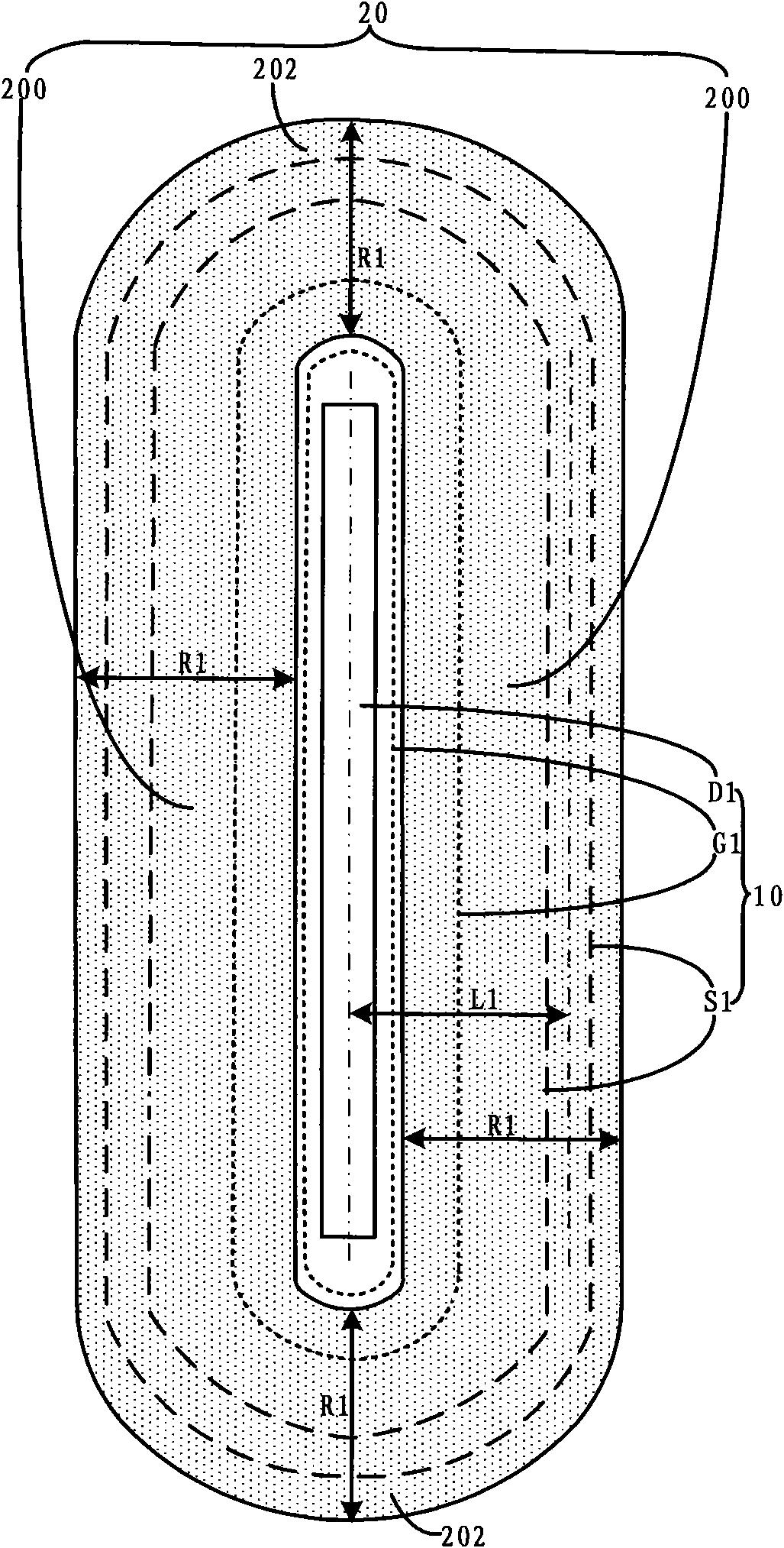
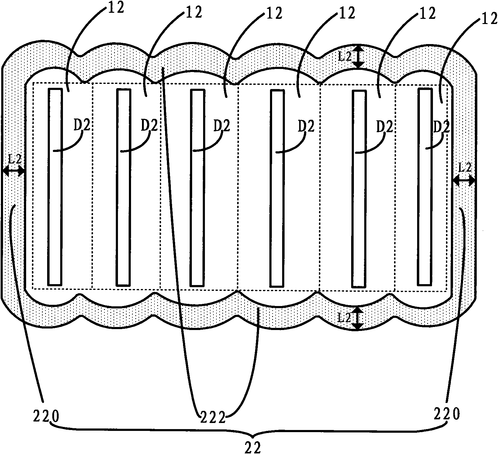
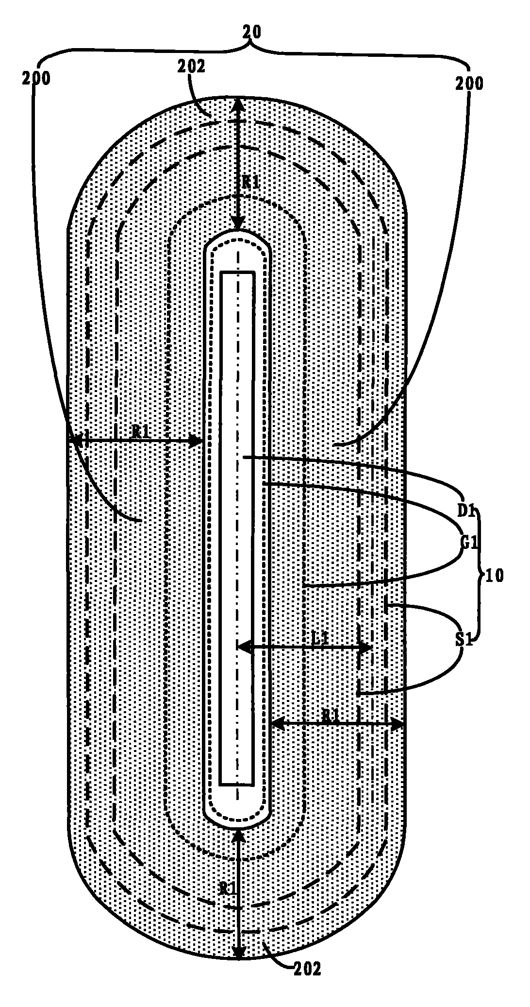
[0017] see figure 1 , which is a schematic diagram of the layout of the first embodiment of the device layout that can improve layout efficiency and integration of the present invention. As shown in the figure, the device layout that can improve layout efficiency and integration of the present invention includes an isolated LDMOS10, The LDMOS10 has a gate G1, a source S1, and a drain D1, and the device layout also includes a first isolation structure 20 surrounding the drain D1, and the ring radius R1 of the first isolation structure 20 is the surrounding drain D1 of the LDMOS10 The distance L1 from the center to the center of the source S1. The first isolation structure 20 includes parallel strips 200 arranged in parallel on both sides of the drain, and an arc-shaped end 202 connected to the end 200 of the parallel strips and f...


PUM


Abstract

The invention provides an element layout capable of increasing layout efficiency and integration degree. In the prior art, elements are separated from one another for a certain distance in order to be insulated from one another, and as a result, the integration degree is low due to a complex design rule and the large insulating distance between the elements. Aimed at an isolated LDMOS, the element layout arranges a first isolating structure around the drain of the isolated LDMOS; aimed at a plurality of LDMOSs connected in parallel, the element layout arranges a second isolating structure around the drains of all the LDMOSs connected in parallel; and the diameters of both the first isolating structure and the second isolating structure are the distance from the center of the surrounded LDMOS drain to the center of the LDMOS source. The invention does not need to design a specific design rule for the isolating structures any more, consequently, the layout process is simplified, the layout efficiency is increased, moreover, the distance between the LDMOSs is reduced, and the integration degree of the elements is increased.

Description

technical field [0001] The invention relates to the field of semiconductor design, in particular to a device layout that can improve layout efficiency and integration. Background technique [0002] In the semiconductor design process, after the logic and circuit design is completed, the layout design can be performed. Layout design is the process of transforming a designed circuit diagram into a specific physical layout. According to logic and circuit function requirements, process level requirements and design rules, a mask layout for lithography is designed. Many design rules need to be defined during layout design, for example, the distance between the source and drain of power MOS transistors with different rated voltages (referred to as device spacing) is different or the size of the drift region of power MOS transistors with different rated voltages is different. [0003] When performing layout design, the insulation design of power MOS tubes operating at high voltage...

Claims


Application Information

Patent Timeline
Patent Type & Authority Applications(China)
IPC IPC(8): G06F17/50
Inventor 刘正超
Owner SHANGHAI HUAHONG GRACE SEMICON MFG CORP
Why Eureka
Try Eureka