VDMOS and preparation method thereof
A manufacturing method and doping layer technology, which is applied in semiconductor/solid-state device manufacturing, electrical components, circuits, etc., can solve problems such as increasing device manufacturing costs, and achieve the effect of increasing manufacturing costs and reducing manufacturing costs
- Summary
- Abstract
- Description
- Claims
- Application Information
AI Technical Summary
Problems solved by technology
Method used
Image

Examples
no. 1 approach
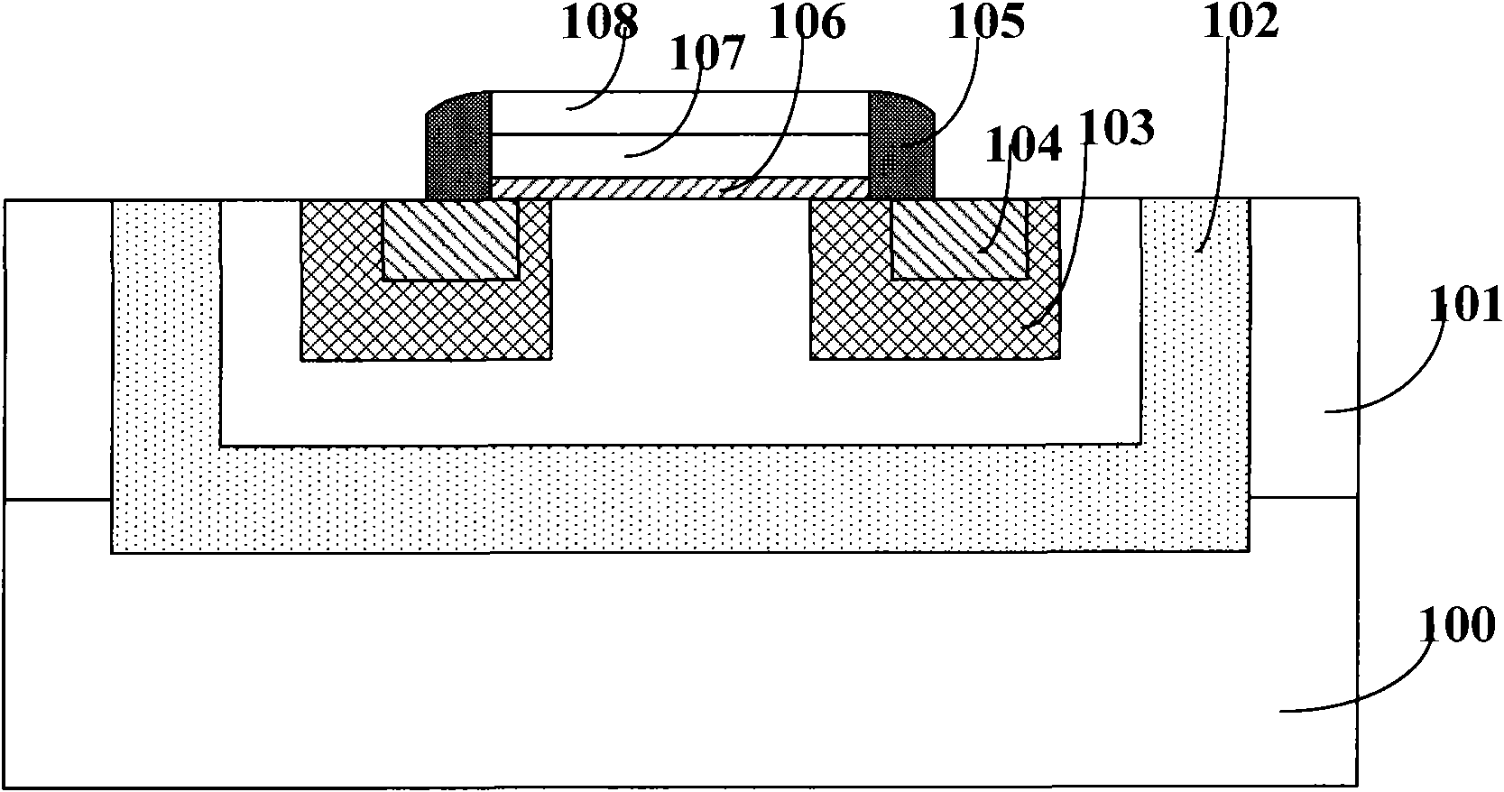
[0016] refer to figure 2 , the present invention at first provides a kind of manufacturing method of VDMOS, comprises the steps:
[0017] Step S11, providing a semiconductor substrate;
[0018] Step S12, forming a doped layer on the base layer in the semiconductor substrate;
[0019] Step S13, forming a gate region on the doped layer; the gate region sequentially includes a gate oxide layer, a polysilicon layer, a silicide layer and sidewalls;
[0020] Step S14, forming isolation wells located on both sides of the gate region in the doped layer;
[0021] Step S15, forming a source region in the isolation well;
[0022] Step S16, forming an opening exposing the base layer in the doped layer;
[0023] Step S17, forming an isolation side wall in the opening;
[0024] Step S18, forming a drain region on the base layer along the opening;
[0025] Step S19, filling the opening with a conductive substance to form a conductive plug.
[0026] The above purpose and the advantage...
no. 2 approach
[0054] refer to Figure 12 , the present invention at first provides a kind of manufacturing method of VDMOS, comprises the steps:
[0055] Step S21, providing a semiconductor substrate;
[0056] Step S22, forming a doped layer on the base layer in the semiconductor substrate;
[0057] Step S23, forming an opening exposing the base layer in the doped layer;
[0058] Step S24, forming an isolation side wall in the opening;
[0059] Step S25, forming a drain region on the base layer along the opening;
[0060] Step S26 , filling the opening with a conductive substance to form a conductive plug.
[0061] Step S27, forming a gate region on the doped layer; the gate region sequentially includes a gate oxide layer, a polysilicon layer, a silicide layer and sidewalls;
[0062] Step S28, forming isolation wells located on both sides of the gate region in the doped layer;
[0063] Step S29, forming a source region in the isolation well;
[0064] first reference Figure 12 with ...
PUM
 Abstract
Description
Claims
Application Information
 - R&D
- Intellectual Property
- Life Sciences
- Materials
- Tech Scout
- Unparalleled Data Quality
- Higher Quality Content
- 60% Fewer Hallucinations
Browse by: Latest US Patents, China's latest patents, Technical Efficacy Thesaurus, Application Domain, Technology Topic, Popular Technical Reports.
© 2025 PatSnap. All rights reserved.Legal|Privacy policy|Modern Slavery Act Transparency Statement|Sitemap|About US| Contact US: help@patsnap.com