Transparent conductive material

A technology of transparent conductors and conductive layers, which is applied in the direction of conductive layers on insulating carriers, electronic equipment, and electrical digital data processing. Prevents cracks and abrasions, achieves durability, and achieves sufficient durability

Inactive Publication Date: 2010-08-04
TDK CORPARATION
View PDF2 Cites 8 Cited by
  • Summary
  • Abstract
  • Description
  • Claims
  • Application Information

AI Technical Summary

Problems solved by technology

[0006] However, in the case of the method of treating the surface of the conductive layer as described above, the durability is improved, but on the other hand, there is a tendency that the resistance value of the electrode surface increases and the conductivity tends to decrease.
Depending on the application, transparent conductors may be required to have a conductive layer with high conductivity, so in this case, it tends to be difficult to maintain high conductivity and improve durability

Method used


Image

  • Transparent conductive material
  • Transparent conductive material
  • Transparent conductive material

Examples


Embodiment 1

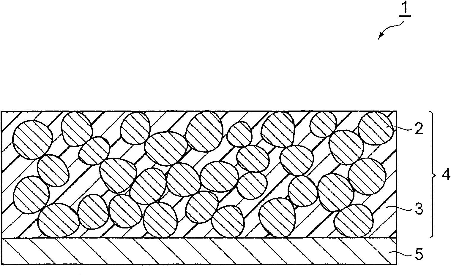
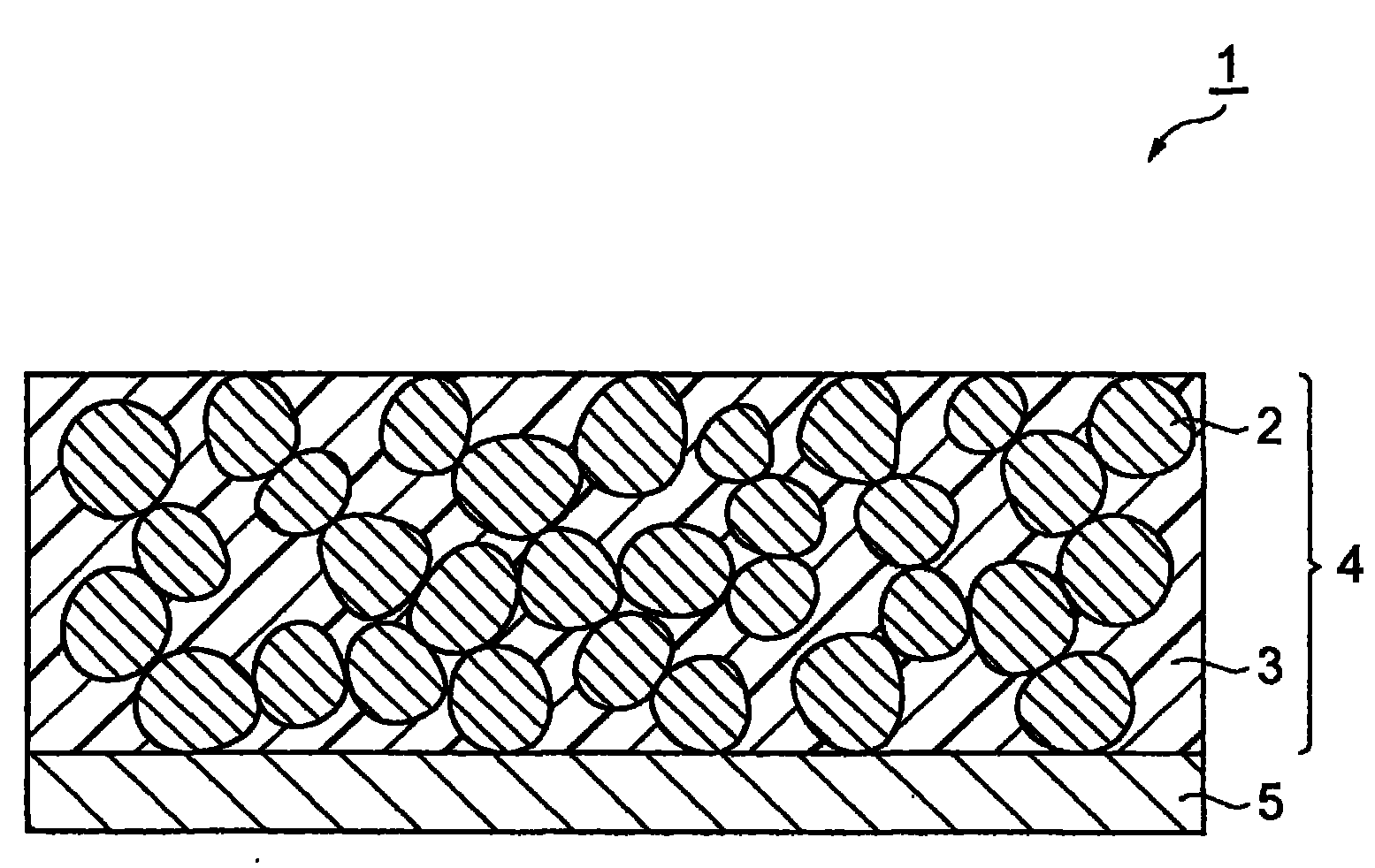
[0074] As a substrate, a polyethylene terephthalate (PET) film (manufactured by TORAY Co., Ltd., thickness: 50 μm) provided with an anchor layer (manufactured by Panasonic Denko Co., Ltd.) in advance was prepared. The ITO dispersion coating solution (the average particle diameter of ITO powder is 30nm, and the solid content concentration is 25%) is coated on this film by bar coating method, and this ITO dispersion coating solution is made of indium oxide doped with tin (hereinafter referred to as "ITO") powder and ethanol. After coating, the ethanol was volatilized, and the ITO powder was fixed on the anchor layer by rolling. Thus, a layer of ITO powder formed by compression on the substrate was formed.

[0075] Next, a solution of the photocurable acrylic resin composition was applied on the layer of the ITO powder by a bar coating method. Here, the solution of the acrylic resin composition was obtained by mixing 20 parts by mass of an acrylic polymer (manufactured by Taise...

Embodiment 2

[0080] A conductive layer was formed in the same manner as in Example 1 above, and after the PET film was peeled off, a fluorinated solvent of 1,1,2,2-tetrahydroperfluorotetradecyltriethoxysilane (manufactured by Gelest) was applied by a bar coating method. The diluted solution (0.05% by mass) was applied on the conductive layer, and the solvent was dried, followed by leaving to stand in an environment of 85° C. and 85% RH for 5 hours. After that, it is immersed in a fluorine solvent to obtain a transparent conductor from which excess fluorine compounds are removed.

Embodiment 3

[0082] Except that the 1,1,2,2-tetrahydroperfluorotetradecyltriethoxysilane (manufactured by Gelest) used in the above Example 2 was changed to 1,1,2,2-tetrahydroperfluoro Except for decyltrichlorosilane, the rest were the same as the above-mentioned Example 2 to prepare a transparent conductor.


PUM

PropertyMeasurementUnit
particle sizeaaaaaaaaaa
specific surface areaaaaaaaaaaa

Abstract

An object of the present invention is to provide a transparent conductive material that can prevent cracks or abrasions on the conductive layer due to repeated use, while maintaining a high conductivity. The transparent conductive material of the present invention has a conductive layer 4 containing a binder 3 and conductive particles 2 held with the binder. In the transparent conductive material, at least a portion of some of the conductive particles 2 is exposed on an outermost surface of the conductive layer, and a fluorine compound is unevenly present on an exposed surface of the conductive particles exposed on the outermost surface of the conductive layer.

Description

technical field [0001] The present invention relates to transparent conductors. Background technique [0002] A panel switch such as a resistive film touch panel (hereinafter referred to as a touch panel) is generally composed of a pair of transparent electrodes facing each other and a spacer sandwiched between the pair of transparent electrodes. If there is a transparent electrode, then the transparent electrode will be in contact with another transparent electrode and energized, thereby detecting the position of its contact point. A transparent conductor is used as the transparent electrode, and the transparent conductor is formed by using a conductive powder and a resin as a conductive layer (see JP-A-11-227740). [0003] When this transparent conductor is used for a touch panel, opposing transparent conductors come into contact with each other, and friction occurs between the transparent conductors. [0004] For this reason, if the touch panel is used repeatedly, crack...

Claims


Application Information

Patent Timeline
Patent Type & Authority Applications(China)
IPC IPC(8): H01B5/14G06F3/045C08J7/044C08J7/046
CPCC08J7/042G06F3/045C08J2367/02B32B7/06B32B27/36C08J7/045B32B27/14B32B27/32B32B27/327B32B27/365B32B2260/025B32B2260/046B32B2264/102B32B2307/202B32B2307/412B32B2307/50B32B2307/546B32B2307/554B32B2307/746B32B2457/208Y10T428/24355C08J7/0423C08J7/046C08J7/044
Inventor 真下倍达安田德行稻叶和久
Owner TDK CORPARATION
Why Eureka
Try Eureka