Organic electroluminescence device and test method thereof

An electroluminescent device and electroluminescent display technology, applied in the direction of electric solid-state devices, electrical components, semiconductor devices, etc., can solve the problem of poor contact or poor contact of chip pins, failure to connect chip pins normally, and failure to light up the light-emitting area And other problems, to achieve the effect of increasing width, high yield and improving life

Active Publication Date: 2010-08-11
SUZHOU QUINGYUE OPTOELECTRONICS TECH CO LTD +1
View PDF5 Cites 21 Cited by
  • Summary
  • Abstract
  • Description
  • Claims
  • Application Information

AI Technical Summary

Problems solved by technology

The over-etched leads are shorter than the length required for bonding, and these over-etched leads cannot be in contact with the corresponding chip pins or have poor contact, resulting in that the corresponding row or column of the light-emitting area cannot be lit
like Figure 2-1 As shown, the leads 201 in the left column and the leads 202 in the right column are over-etched, and their length is shorter than the length required for bon

Method used


Image

  • Organic electroluminescence device and test method thereof
  • Organic electroluminescence device and test method thereof
  • Organic electroluminescence device and test method thereof

Examples


Embodiment 1

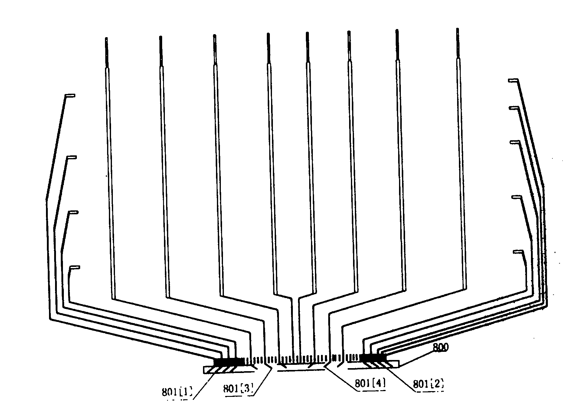
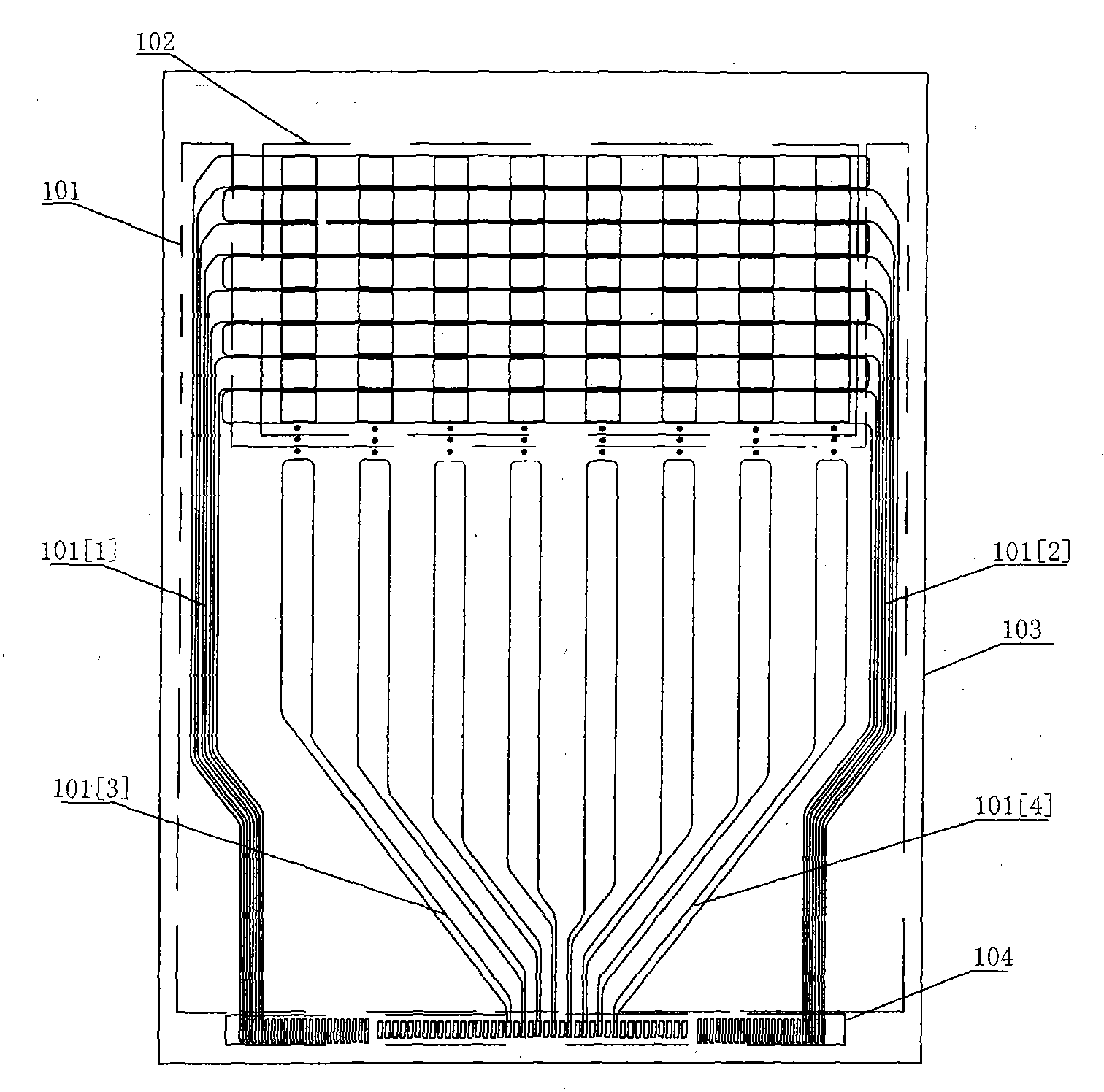
[0043] Such as image 3 , Figure 4 As shown, Embodiment 1 is an organic electroluminescent device with 96 rows×16 columns.

[0044] The odd-numbered row leads 401[1] and even-numbered row leads 401[2] are drawn out horizontally from the light-emitting area, and the left column leads 401[3] and right column leads 401[4] are drawn longitudinally. The ends of the leads are located at the lead extension 300 . After the lead 401[3] in the left column is bonded to the chip pin, its end extends to the left at 30° from the vertical direction after exceeding the chip pin; after the lead 401[4] in the right column is bonded to the chip pin, its end After the end exceeds the chip pins, it extends to the right at 30° from the vertical direction; after the odd-numbered row leads 401[1] are bonded to the chip pins, their ends exceed the chip pins and extend to the right at 30° from the vertical direction Extension: After the even-numbered row leads 401[2] are bonded to the chip pins, th...

Embodiment 2

[0053] Such as Figure 5 As shown, Embodiment 2 is also an organic electroluminescent device with 96 rows×16 columns. The odd-numbered row leads 501[1] and even-numbered row leads 501[2] are drawn laterally from the light-emitting area, and the left column leads 501[3] and right column leads 501[4] are drawn longitudinally. The ends of the leads are located at the lead extension 500 . After the left column lead 501[3] is bonded to the chip pin, its end extends to the left at 45° from the vertical direction after exceeding the chip pin; after the right column lead 501[4] is bonded to the chip pin, its end After the end exceeds the chip pins, it extends to the right at 45° from the vertical direction; after the odd-numbered row leads 501[1] are bonded to the chip pins, their ends exceed the chip pins and extend to the left at 45° from the vertical direction Extension: After the even-numbered row leads 501[2] are bonded to the chip pins, their ends extend to the right at 45° fr...

Embodiment 3

[0057] Such as Figure 6 , Figure 7 As shown, Embodiment 3 is an organic electroluminescent device with 64 rows×128 columns. The odd-numbered row leads 701[1] and even-numbered row leads 701[2] are drawn laterally from the light-emitting area, and the left column leads 701[3] and right column leads 701[4] are drawn longitudinally. The ends of the leads are located at the lead extension 700 . After the left-column lead 701[3] is bonded to the chip pin, its end extends to the right at 60° from the vertical direction after exceeding the chip pin; after the right-column lead 701[4] is bonded to the chip pin, its end After the end exceeds the chip pins, it extends to the left at 60° from the vertical direction; after the odd-numbered row leads 701[1] are bonded to the chip pins, their ends exceed the chip pins and extend to the right at 60° from the vertical direction Extension: After the even-numbered row leads 701[2] are bonded to the chip pins, their ends extend to the left ...


PUM


Abstract

The invention discloses an organic electroluminescence device and a test method thereof. The organic electroluminescence device comprises a luminescent area, a lead wire area and a bonding area. The luminescent area comprises an anode, a organic functional layer and a cathode; the lead wire area consists of a lead wire connecting the anode and the cathode with a driving chip or a circuit board; the bonding area is an area in which the lead wire is connected with the driving chip or the circuit board, wherein a lead wire elongation area is comprised, the end of the lead wire is located in the lead wire elongation area, and the lead wire in the lead wire elongation area and the lead wire in the lead wire area are in parallel or form a certain angel. The invention changes the lead wire arrangement of the OLED. Therefore the conductive adhesive tape can be more easily and accurately in compression connection with the lead wire, and simultaneously prevent the procession lead wire from short circuit during the test phase of the screen body.

Description

technical field [0001] The invention relates to an organic light emitting device (Organic Light Emitting Device, referred to as OLED hereinafter) and a testing method thereof, in particular to the lead design of the OLED. Background technique [0002] OLED is a flat-panel display device made by using the phenomenon that carriers enter the organic functional layer from the anode and cathode to recombine and emit light under the action of an electric field. OLED has the characteristics of all solid state, self-illumination, high contrast, ultra-thin, and flexible display. [0003] The current electronic devices have to go through testing and aging before leaving the factory to test the performance of the devices. Corresponding to different chip bonding technologies, different problems will arise during the testing and burn-in phase. Use COG (Chip on glass) method to bond the screen body and chip, refer to Picture 1-1 and Figure 1-2 , OLED includes a substrate 103 and a li...

Claims


Application Information

Patent Timeline
IPC IPC(8): H01L27/32H01L23/528G01R31/00
Inventor 邱勇彭兆基钟馨义孙剑
Owner SUZHOU QUINGYUE OPTOELECTRONICS TECH CO LTD
Why Eureka
Try Eureka