Input buffer circuit for high-speed pipeline analog-to-digital converter

A technology of input buffers and analog-to-digital converters, applied in the direction of analog-to-digital converters, can solve problems such as low gain, input and output errors, and reduce the spurious-free dynamic range of input signals, so as to reduce load capacitance and increase Effect of Output Impedance

Inactive Publication Date: 2010-08-11
ZHEJIANG UNIV
View PDF2 Cites 15 Cited by
  • Summary
  • Abstract
  • Description
  • Claims
  • Application Information

AI Technical Summary

Problems solved by technology

[0008] However, the biggest disadvantage of circuit 100 and circuit 101 is that the gain is relatively low, because usually the gain of a common single-stage operational amplifier is below 40dB, and if the quiescent current is increased in order to meet the high-speed requirements, the gain will be lower, so in the closed loop In the system application, it will lead to a relatively large error in the input and output, which will reduce the spurious-free dynamic range (SFDR) of the input signal

Method used


Image

  • Input buffer circuit for high-speed pipeline analog-to-digital converter
  • Input buffer circuit for high-speed pipeline analog-to-digital converter
  • Input buffer circuit for high-speed pipeline analog-to-digital converter

Examples


Embodiment Construction

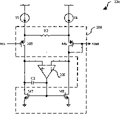
[0026] In any electronic communication system, if fast digital processing of analog signals is required, then a high-speed analog-to-digital converter is required as an interface, and the input buffer circuit of the present invention can be integrated in any analog-to-digital processing that needs to process high-speed signals. Inside the converter, such as the input buffer at the front end of a high-speed pipeline ADC.

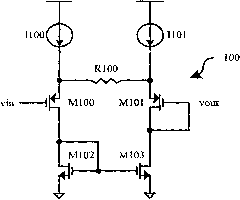
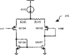
[0027] As mentioned earlier, the traditional source-level negative feedback amplifiers, shown as 100 and 101 in Figure 1, have relatively good linearity, but due to the low gain, there will be a relatively large gap between the closed-loop output and input. error. Moreover, as the frequency of the input signal increases, the SFDR of the output signal will drop more severely. Such an input buffer does not meet the requirements of the front-end circuit of the high-speed analog-to-digital converter, because the high-speed ADC usually needs to under-sample the input...


PUM


Abstract

The invention provides a input buffer circuit for high-speed pipeline analog-to-digital converter (ADC). The input buffer circuit comprises an input pair transistor, a current mirror load, a gain-boosted amplifier and a compensation capacitor, wherein the input pair transistor consists of a first MOS (metal oxide semi-conductor) transistor and a second MOS transistor of a source negative-feedback resistor; the current mirror load consists of a third MOS transistor and a fourth transistor which are connected to each other by a gate; the positive input terminal of the gain-boosted amplifier is connected with the drain of the first MOS transistor, the negative input terminal thereof is connected with the drain of the second MOS transistor, and the output terminal thereof is connected with the gate of the third MOS resistor; and one terminal of the compensation capacitor is connected with the gate of the third MOS transistor, and the other terminal thereof is connected with the drain of the third MOS transistor. The input buffer circuit of the invention is capable of meeting the requirements for the input of high-speed signals, effectively reducing the inputted load capacitance and increasing the outputted impedance.

Description

Technical field [0001] The invention relates to an integrated circuit used in the field of communication technology, and in particular to an input buffer circuit of a high-speed analog-to-digital converter. Background technique [0002] With the rapid development of the communications industry, various electronic devices are being widely used, such as mobile phones, computers, MP4 and so on. In these electronic devices, the analog-to-digital converter has become indispensable as an interface circuit for analog signals and digital signals, and its applications are increasing. In order to process video signals, the analog-to-digital converters used in some electronic devices require high speed, which puts higher requirements on the input bandwidth and linearity of the analog-to-digital converters. The usual approach is to make an ADC drive circuit outside the ADC chip. Such drive circuit is generally a closed-loop amplifier, but this not only requires an additional amplifier, but ...

Claims


Application Information

Patent Timeline
Patent Type & Authority Applications(China)
IPC IPC(8): H03M1/12
Inventor 张鲁何乐年
Owner ZHEJIANG UNIV
Why Eureka
Try Eureka