Manufacturing apparatus for semiconductor device, controlling method for manufacturing apparatus, and storage medium storing control program for manufacturing apparatus

A technology of a manufacturing device and a control method, which is applied in semiconductor/solid-state device manufacturing, photolithography process exposure devices, electrical components, etc., can solve problems such as pattern size differences, actual exposure differences, etc., and achieve the effect of suppressing deviations

Inactive Publication Date: 2010-08-18
NEC ELECTRONICS CORP
View PDF6 Cites 0 Cited by
  • Summary
  • Abstract
  • Description
  • Claims
  • Application Information

AI Technical Summary

Problems solved by technology

However, the exposure sensor has a separate change
Individual changes in the exposure sensor can result in differences in actual exposure across multiple exposure stations
There is a problem that such a difference in the amount of exposure causes a difference in the size of the pattern formed among the exposure stages

Method used


Image

  • Manufacturing apparatus for semiconductor device, controlling method for manufacturing apparatus, and storage medium storing control program for manufacturing apparatus
  • Manufacturing apparatus for semiconductor device, controlling method for manufacturing apparatus, and storage medium storing control program for manufacturing apparatus
  • Manufacturing apparatus for semiconductor device, controlling method for manufacturing apparatus, and storage medium storing control program for manufacturing apparatus

Examples


Embodiment Construction

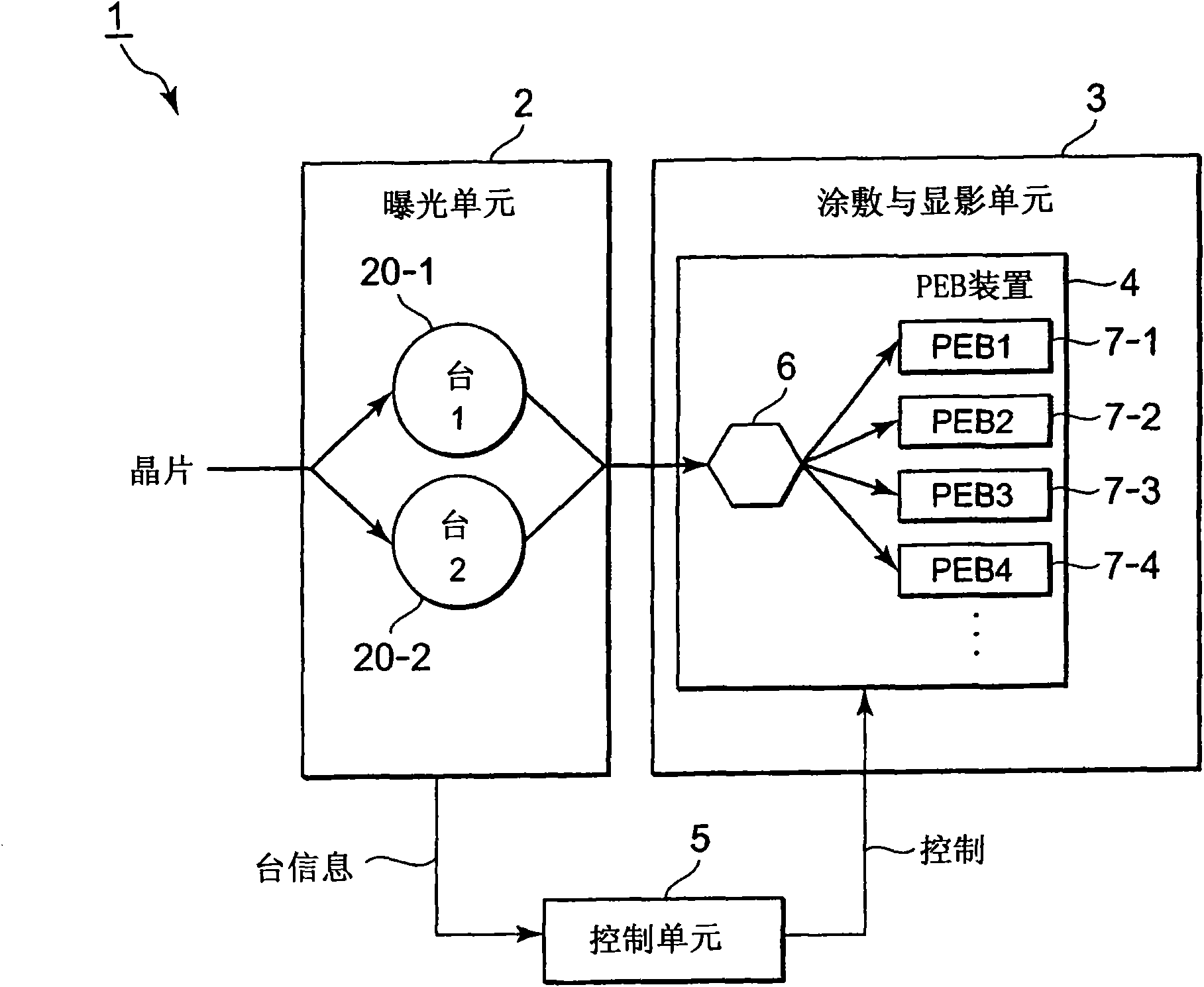
[0023] Hereinafter, embodiments of the present invention are described with reference to the drawings. figure 1 is a configuration diagram showing the semiconductor device manufacturing apparatus 1 according to this embodiment.

[0024] Such as figure 1 As shown, the semiconductor device manufacturing apparatus 1 includes an exposure unit 2 , a coating and developing unit 3 and a control unit 5 . The coating and developing unit 3 includes a post exposure bake (PEB) device 4 (heating device) and a developing device (not shown).

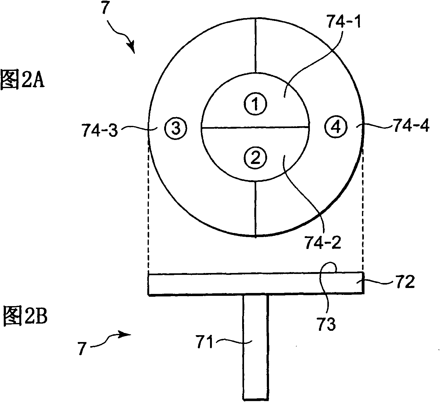
[0025] The exposure unit 2 is a device for exposing a wafer on which a resist film is formed. In general, the exposure unit 2 exposes (to light) a resist film formed on a wafer through a photomask on which a predetermined pattern (so as to include transparent portions and opaque portions) is formed. As the resist, a chemically amplified resist is used. The exposure unit 2 has a plurality (two) of exposure stages 20 (20-1 and 20-2). Each exposure s...


PUM


Abstract

The manufacturing apparatus for a semiconductor device includes: a stage information obtaining portion for obtaining stage information that is information for specifying an exposure stage used in an exposure process of a wafer to be heated from an exposure unit including a plurality of exposure stages on which the wafer is placed; and a temperature setting portion for setting heating temperature of a heating apparatus for heating the wafer to be heated. The temperature setting portion sets the heating temperature based on the stage information individually for each of the plurality of exposure stages.

Description

technical field [0001] The present invention relates to a manufacturing apparatus of a semiconductor device, a control method for the manufacturing apparatus, and a storage medium storing a control program for the manufacturing apparatus. Background technique [0002] When manufacturing a semiconductor device, it is desirable to form a pattern whose size exactly matches a target size. However, when manufacturing a semiconductor device, there are various factors that cause dimensional deviations in formed patterns. [0003] As a factor causing pattern size deviation, there is heating temperature in a post-exposure bake (PEB) process. When manufacturing a semiconductor device, a resist film made of resin is formed on a film to be processed of a wafer. Then, the resist film is exposed through a photomask forming a predetermined pattern. The exposed wafer is heated. This heating process is performed to accelerate the chemical reaction of the resist film, and is called a post...

Claims


Application Information

Patent Timeline
Patent Type & Authority Applications(China)
IPC IPC(8): H01L21/00H01L21/027G03F7/20
CPCH01L21/67248
Inventor 村上贵
Owner NEC ELECTRONICS CORP
Why Eureka
Try Eureka