

CMOS (Complementary Metal Oxide Semiconductor) image sensor
An image sensor and pixel unit technology, applied in the field of image sensors, can solve the problems of limited bandwidth of negative feedback operational amplifier A and limited effect of eliminating reset noise, etc., and achieve the effect of ensuring removal of reset noise, reduction of reset noise, and stable voltage
- Summary
- Abstract
- Description
- Claims
- Application Information
AI Technical Summary
Problems solved by technology
Method used
Image

Examples
no. 1 example
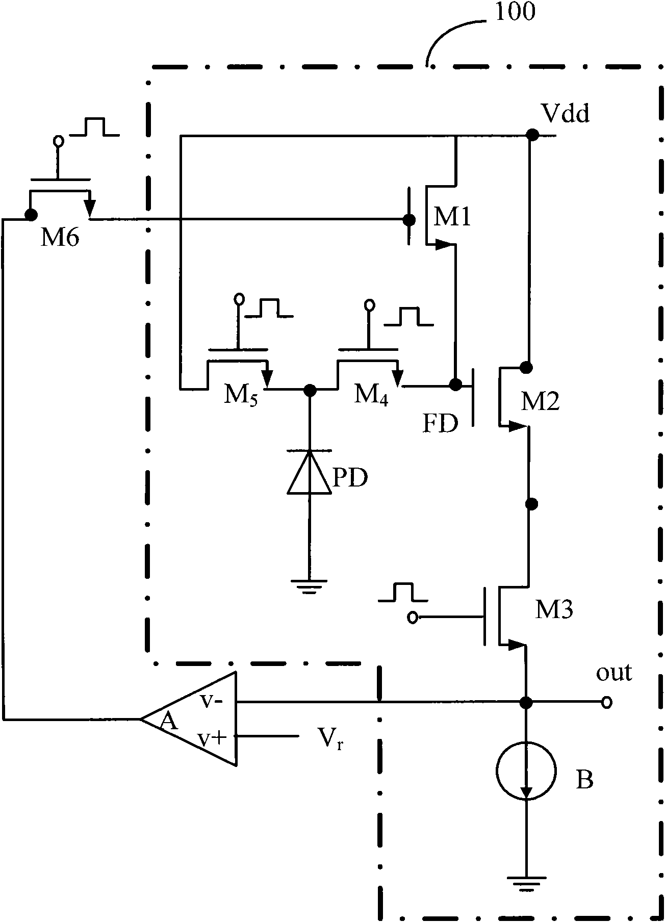
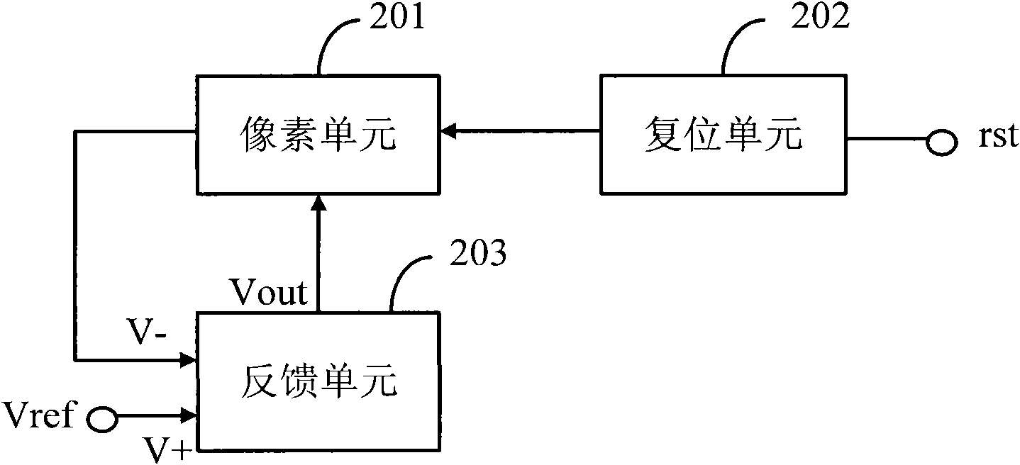
[0042] Please refer to FIG. 3 , which is a schematic circuit diagram of a 3T CMOS image sensor according to a first embodiment of the present invention. The CMOS image sensor includes a pixel unit 201 , a feedback unit 203 and a reset unit 202 . The 3T type CMOS image sensor in the present invention specifically means that the pixel unit 201 includes one photodiode and three NMOS transistors, namely: photodiode PD, reset transistor M1, amplifier transistor M2, and selection transistor M3. The reset transistor M1 has a source, and the source is called the sensing node FD of the pixel unit by those skilled in the art.
[0043] Continuing to refer to FIG. 3 , the feedback unit 203 includes a negative feedback operational amplifier A, and the negative feedback operational amplifier A includes an input negative terminal V - , input positive terminal V + and the output V out , the input negative terminal V - electrically connected to the source of select transistor M3, the input...
no. 2 example
[0073] FIG. 5 is a schematic diagram of a circuit structure of a 4T CMOS image sensor according to a second embodiment of the present invention.
[0074] The CMOS image sensor includes a pixel unit 201 , a feedback unit 203 and a reset unit 202 . The 4T type CMOS image sensor described in the present invention specifically means that the pixel unit 201 includes 1 photodiode and 4 NMOS transistors, which are respectively: photodiode PD, reset transistor M1, amplification transistor M2, selection transistor M3, transfer transistor M4. The reset transistor M1 has a source, which is referred to as a sensing node FD of the pixel unit 201 by those skilled in the art.
[0075] Referring to Fig. 5, as a preferred embodiment, the CMOS image sensor also includes:
[0076] The first switch K1, the drains of the amplifying transistor M2 and the reset transistor M1 are electrically connected to the output end of the feedback unit 203 through the first switch K1, the first switch K1 recei...
no. 3 example
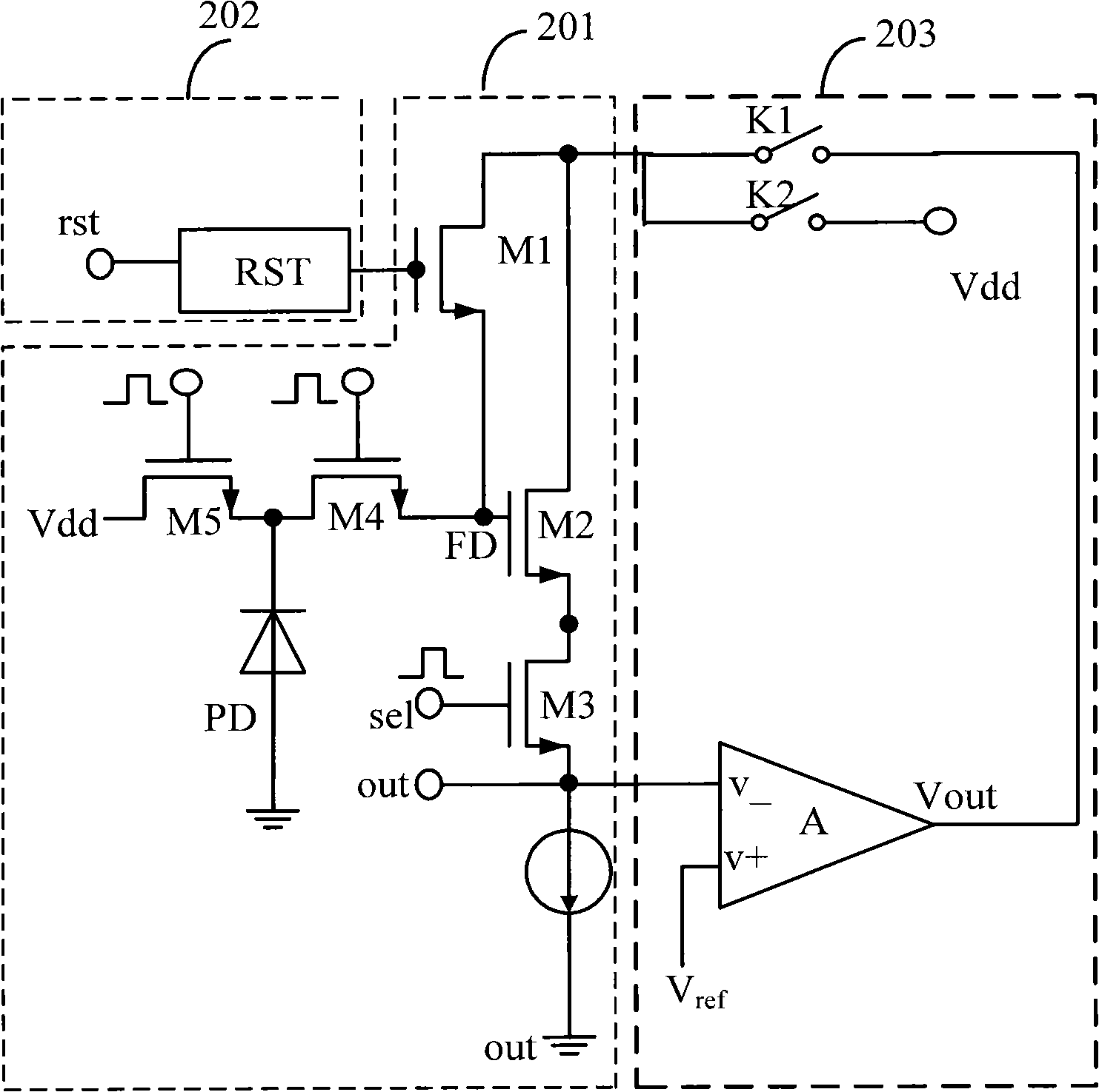
[0088] Please refer to FIG. 6 , which is a schematic circuit diagram of a 5T CMOS image sensor according to a third embodiment of the present invention. The CMOS image sensor includes a pixel unit 201 , a control unit 202 and a feedback unit 203 . The 5T type CMOS image sensor in the present invention refers to that the pixel unit 201 includes 1 photodiode and 5 NMOS transistors, which are respectively: photodiode PD, reset transistor M1, amplification transistor M2, selection transistor M3, transfer transistor M4, global Reset transistor M5. The reset transistor M1 has a source, and the source is called the sensing node FD of the pixel unit by those skilled in the art.
[0089] As a preferred embodiment, the CMOS image sensor also includes:
[0090] The first switch K1, the drains of the amplifying transistor M2 and the reset transistor M1 are electrically connected to the output end of the feedback unit 203 through the first switch K1, the first switch K1 receives the cont...
PUM
 Abstract
Description
Claims
Application Information