
Gate driving circuit

A gate drive circuit and circuit technology, applied in electrical components, electronic switches, adjusting electrical variables, etc., to achieve the effect of reducing raw materials, efficient thermal design, and suppressing the deviation of conduction loss

Inactive Publication Date: 2013-04-03
MITSUBISHI ELECTRIC CORP
View PDF4 Cites 2 Cited by
  • Summary
  • Abstract
  • Description
  • Claims
  • Application Information

AI Technical Summary

Problems solved by technology

[0004] In the conventional gate drive circuit, there is a limitation in the rising speed of the constant current circuit when the insulated gate transistor is turned on, so the current at the gate terminal cannot be immediately become a constant value
In addition, in the current value switching of the constant current circuit, a switch is used in series with the constant current circuit, and the constant current circuit must increase the current to a predetermined current value from a non-operating state, so the rise of the constant current may be slow.
Therefore, if the threshold voltage (VGEth) of the gate terminal varies, the conduction loss will vary, so there is a problem that thermal design with a large margin is necessary, and efficient thermal design cannot be performed.

Method used


Image

  • Gate driving circuit
  • Gate driving circuit
  • Gate driving circuit

Examples


Embodiment approach 1

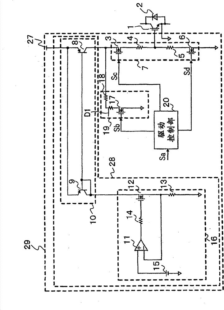
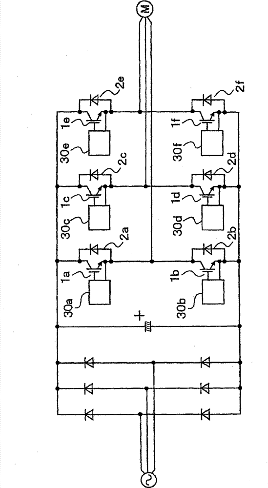
[0030] figure 1 It is a circuit diagram of the gate drive circuit in Embodiment 1 of this invention. As the semiconductor element 1 for power, an IGBT1 (Insulated Gate Bipolar Transistor, insulated gate bipolar transistor) is used. However, not limited to IGBTs, even if they are composed of other switches such as FET (Field Effect Transistor) or switches using not only silicon but also other materials such as silicon carbide (SiC) and gallium nitride (GaN), the same The effect is self-evident. The combination of IGBT1, diode 2, and gate drive circuit 29 described here can be used for example figure 2 In various power converters such as the 3-phase inverter circuit shown.

[0031] exist figure 2 Among them, 1a to 1f represent power semiconductor devices (IGBTs), 2a to 2f represent diodes, and 30a to 30f represent gate drive circuits. The gate drive circuits 30a to 30f control the switching of the power semiconductor elements 1a to 1f with respect to the current obtained...

Embodiment approach 2

[0049] Figure 6 It is a circuit diagram showing a gate drive circuit according to Embodiment 2 of the present invention. exist Figure 6 In , the same or related symbols are used to denote the same or equivalent parts as those in the above-mentioned embodiment, and description thereof will be omitted. exist Figure 6 In the gate drive circuit 29a, the preliminary energization circuit 19a is connected to the gate terminal of the IGBT1, and the preliminary energization circuit 19a is composed of an N-channel MOSFET 17a and a resistor 18a as a second switch for controlling the current to the gate terminal of the IGBT1. constitute. The drain of N-channel MOSFET 17a is connected to the gate terminal of IGBT1 via resistor 18a, the gate is connected to drive control unit 20, and the source is connected to the ground side.

[0050] Figure 7 shown for illustration Figure 6 Timing diagram of the operation of the circuit. Figure 7 (a) shows the control command signal Sa, (b) s...

Embodiment approach 3

[0056] Figure 8 It is a circuit diagram of a gate drive circuit according to Embodiment 3 of the present invention. exist Figure 8In , the same or corresponding parts as those in the above-mentioned embodiment are denoted by the same or related symbols, and explanations thereof are omitted. exist Figure 8 In the gate drive circuit 29b, the constant current circuit 16a is usually set to a small current, and is set to a large current only when necessary. Therefore, a resistor 23 is connected in series with the setting resistor 13 for setting the constant current value of the constant current circuit 16a, and a switch 24 for short-circuiting both ends of the resistor 23 is connected in parallel with the resistor 23. Furthermore, comparators 22 and 26 are provided, and the comparators 22 and 26 are connected to the gate terminal of the IGBT 1 and compare the gate voltage with a preset voltage.

[0057] The first reference power source 21 that generates the first reference v...


PUM


Abstract

To obtain a gate driving circuit in which rising of a constant current of a constant current circuit is fast and power saving is achieved, the gate driving circuit includes: a constant current driving circuit (28) for supplying a constant current; a gate terminal of a power semiconductor element (1), which is connected to an output terminal of the constant current driving circuit; a comparator (22) for comparing a voltage at the gate terminal with a predetermined voltage value and outputting a signal indicating that the voltage is higher than the predetermined voltage value; and a driving control section (20) for increasing a current from the constant current driving circuit (28) in response to a signal for turning on the power semiconductor element (1), and reducing the current from the constant current driving circuit (28) in response to the signal from the comparator (22).

Description

technical field [0001] The present invention relates to a gate drive circuit for driving power semiconductor elements. Background technique [0002] In a conventional gate drive circuit of a power semiconductor element in a load driving device, a constant current circuit and a current mirror circuit are used to drive a constant current through a gate terminal in order to drive an insulated gate transistor. In addition, in order to switch the current value of the constant current circuit, a switch is used in series with the constant current circuit (for example, refer to Patent Document 1). [0003] Patent Document 1: Japanese Patent Application Laid-Open No. 2003-318713 (Fig. 1) [0004] In the conventional gate drive circuit, when the insulated gate transistor is turned on, the rising speed of the constant current circuit is limited, so the current at the gate terminal cannot immediately become a constant value. In addition, in switching the current value of the constant...

Claims


Application Information

Patent Timeline
Patent Type & Authority Patents(China)
IPC IPC(8): H02M1/08
CPCH03K17/0412H03K17/162H03K17/0406H02M1/08H03K2217/0036G05F3/26
Inventor 中武浩福优奥田达也角田义一
Owner MITSUBISHI ELECTRIC CORP
Learn More