Gluing device, use method and products thereof

A glue coating device and product technology, which is applied to the surface coating liquid device, coating, semiconductor/solid device manufacturing, etc., can solve the problem of uneven thickness of the glue, air in the glue, and large resistance of the glue flowing through the scraper, etc. question

Inactive Publication Date: 2010-09-08
D TEK TECHNOLOGY CO LTD
View PDF1 Cites 28 Cited by
  • Summary
  • Abstract
  • Description
  • Claims
  • Application Information

AI Technical Summary

Problems solved by technology

When the scraper of this shape is coating the colloid, the resistance of the colloid to flow through the scraper is relatively large, so sometimes the thickness of the colloid is uneven, or the colloid contains air, etc.

Method used


Image

  • Gluing device, use method and products thereof
  • Gluing device, use method and products thereof
  • Gluing device, use method and products thereof

Examples


Embodiment Construction

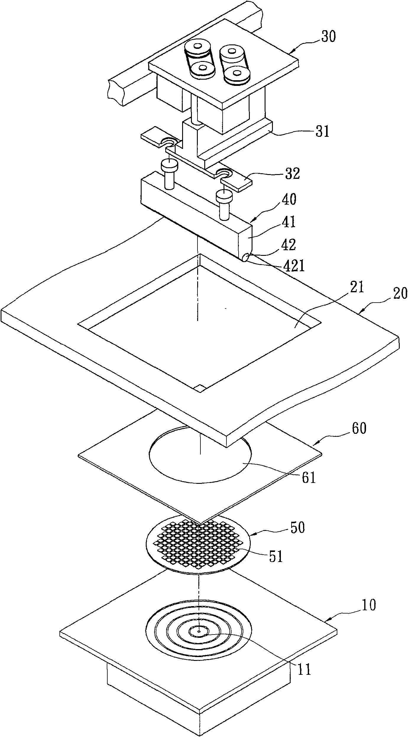
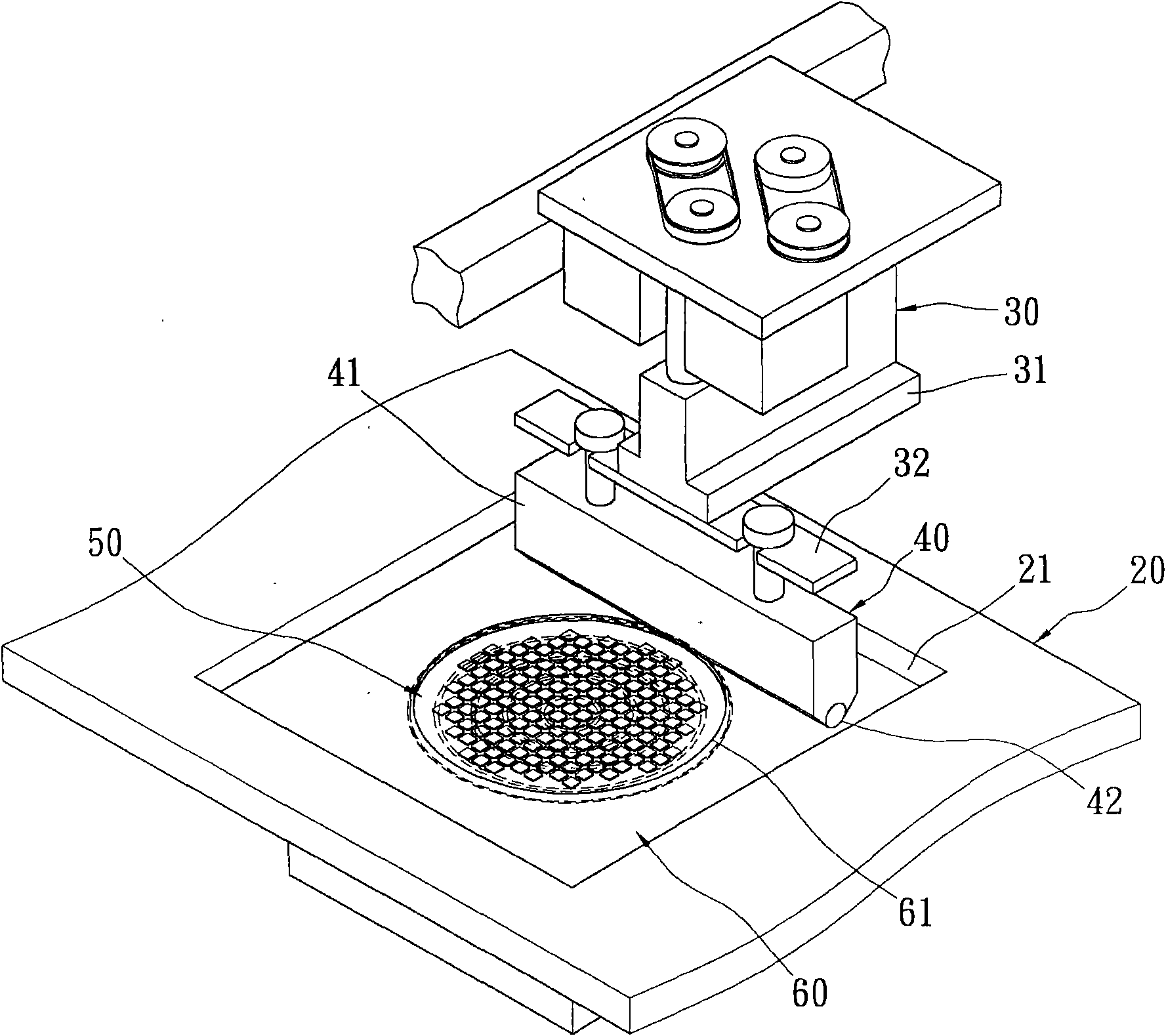
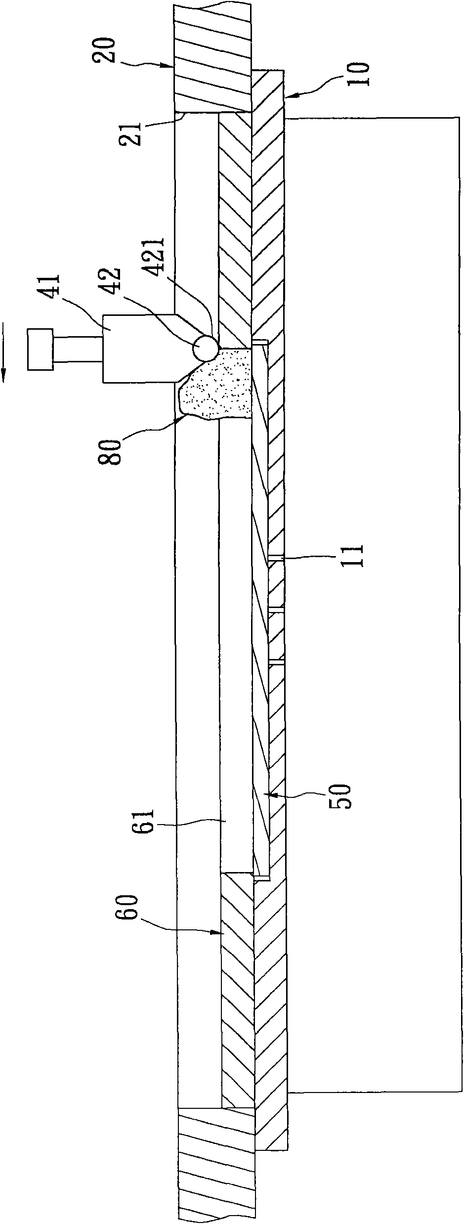
[0043] see Figure 1 to Figure 3 , the present invention proposes a gluing device, which includes: a vacuum chuck 10 , a placement platform 20 , a scraper moving module 30 and a scraper structure 40 .

[0044] The vacuum chuck 10 is a board, which can move up and down to change the use height of the vacuum chuck 10 . The center of the vacuum chuck 10 has a plurality of suction holes 11 . The suction holes 11 are recessed on the top surface of the vacuum chuck 10 and penetrate to the bottom surface of the vacuum chuck 10 . The vacuum chuck 10 also has a vacuum pump (not shown), and the lower end of the suction hole 11 is connected with the vacuum pump. Thus, when the vacuum pump generates suction, the suction hole 11 will also generate suction to absorb an object to be glued 50 (such as a wafer) placed on the top surface of the vacuum chuck 10 .

[0045] The placing platform 20 is arranged on the top of the vacuum chuck 10, and has a rectangular placing groove 21 in its cente...


PUM


Abstract

The invention relates to a gluing device, a use method and products thereof. The gluing device comprises a vacuum cup, a platform arranged above the vacuum cup, a scraper moving module arranged above the platform movably and a scraper structure arranged on one end of the scraper moving module. The tail end of the scraper structure is an arc surface. The steps of the use method of the gluing device are as follows: putting an objected to be glued on the vacuum cup; putting one steel plate or one screen on the platform; setting glue in a pre-calculated volume on one side of the steel plate or screen; and then moving the scarper structure to drive the glue from one side of the steel plate or screen to the other side so as to coat the glue on the object to be glued. Since the scraper structure has the arc surface, the invention can coat the glue on the object to be glued smoothly.

Description

technical field [0001] The invention relates to a gluing device, its use method and its products, in particular to a gluing device with a scraper structure, its use method and its products. Background technique [0002] After the general wafer (wafer) is made into an integrated circuit chip (integrated circuit chip, IC chip), it will further use a glue coating machine (printing machine) to coat a layer of glue on the upper or lower surface of the wafer. or glue). Then, after the colloid is slightly dried, the wafer is cut into a plurality of circuit chips. The chip is bonded to a substrate or another chip respectively, and after the colloid is completely dried and solidified, the chip and the substrate or another chip can be fixedly bonded together. "A Wafer Coating Structure for Chip Packaging (1)" proposed by Taiwan Patent Certificate No. M3262839 discloses this technology. After the chip and the substrate (chip and chip) are combined, some chip packaging operations suc...

Claims


Application Information

Patent Timeline
Patent Type & Authority Applications(China)
IPC IPC(8): B05C9/02B05C11/04B05C13/02H01L21/56H01L21/58
Inventor 费耀祺
Owner D TEK TECHNOLOGY CO LTD
Why Eureka
Try Eureka