Method for manufacturing black silicon material by scanning and irradiation of light source of broad-pulse laser

A laser and wide-pulse technology, which is applied in the field of scanning and irradiating black silicon materials with wide-pulse laser light sources. The effect of shortening the time of the same area, cheap price, and wide working pulse width

Inactive Publication Date: 2012-03-28
INST OF SEMICONDUCTORS - CHINESE ACAD OF SCI
View PDF0 Cites 0 Cited by
  • Summary
  • Abstract
  • Description
  • Claims
  • Application Information

AI Technical Summary

Problems solved by technology

[0005] At present, in the black silicon material production technology that has been disclosed, the laser light source used is a narrow pulse femtosecond laser light source with a wavelength of ≤800nm. The wavelength of the light source is much smaller than the band gap wavelength of the silicon material, so that the effect of light on silicon within a few micrometers of silicon surface thickness
[0006] In addition, the high-power narrow-pulse femtosecond laser source used has a complex structure and high price, which is not conducive to the industrial production of black silicon materials

Method used


Image

  • Method for manufacturing black silicon material by scanning and irradiation of light source of broad-pulse laser
  • Method for manufacturing black silicon material by scanning and irradiation of light source of broad-pulse laser

Examples


Embodiment Construction

[0024] In order to make the object, technical solution and advantages of the present invention clearer, the present invention will be described in further detail below in conjunction with specific embodiments and with reference to the accompanying drawings.

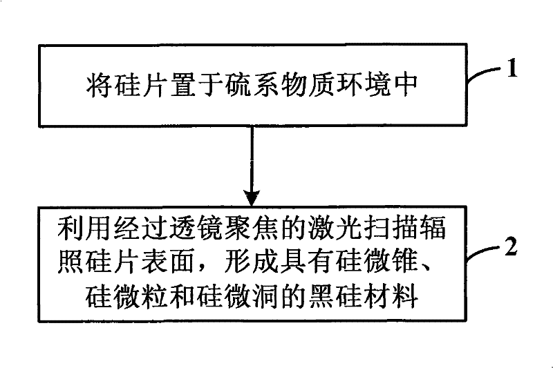
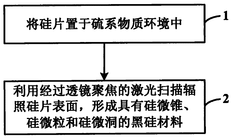
[0025] The method provided by the present invention adopts wide pulse laser light source scanning irradiation to produce black silicon material, the pulse width is from nanoseconds or microseconds or milliseconds to continuous DC mode, and the wavelength is 1064nm. Using this kind of wide pulse 1064nm laser light source to scan a silicon wafer placed in a chalcogenide environment can produce silicon microcones, particles, and microcavity microstructures on the surface of the wafer to form a so-called black silicon material, which is harmful to the sun. The spectrum has a strong absorption coefficient and is not limited by the low-energy absorption band of silicon, even in the near-infrared band of the solar spectrum, it st...


PUM

PropertyMeasurementUnit
lengthaaaaaaaaaa
widthaaaaaaaaaa
heightaaaaaaaaaa

Abstract

The invention discloses a method for manufacturing a black silicon material by scanning and irradiation of a light source of a broad-pulse laser, comprising the following steps of: 1, putting silicon slices into a sulfur-series matter environment; and 2, scanning and irradiating the surfaces of the silicon slices by using lasers focused through a lens to form the black silicon material with silicon micro tapers, silicon micro particles and silicon micro holes. By using the method, the used laser pulse width is in a nanosecond or microsecond or millisecond mode, even a continuous direct-current mode, and the wavelength is 1064 nm. The black silicon micro-structure material with silicon micro tapers, silicon micro particles and silicon micro holes, which has strong absorb function for a whole solar spectrum, can be manufactured by using the light source of the broad-pulse laser to scan the silicon slices in the sulfur-series matter environment.

Description

technical field [0001] The invention relates to the technical field of semiconductor optoelectronic materials, in particular to a method for producing black silicon material by scanning and irradiating a wide pulse laser light source. Background technique [0002] In recent years, material surface processing technology based on high-intensity laser scanning irradiation has received extensive attention. Researchers at Harvard University in the United States scanned the silicon surface with a high-intensity femtosecond laser light source, and obtained a new material with a fine-sized pyramid-conical microstructure, the so-called black silicon material. [0003] The light absorption efficiency of black silicon material is significantly improved (MRS Belletin, 31 (2006) 594). Especially when silicon wafers are exposed to chalcogenide gases such as SF 6 , H 2 Under S and other environments, the black silicon material obtained after laser light source scanning has an absorption...

Claims


Application Information

Patent Timeline
Patent Type & Authority Patents(China)
IPC IPC(8): C30B33/00C30B31/20H01L31/0288H01L31/102
Inventor 梁松朱洪亮林学春韩培德王宝华
Owner INST OF SEMICONDUCTORS - CHINESE ACAD OF SCI
Why Eureka
Try Eureka