Separation testing method of pixel of electric testing point and testing device thereof

A test method and technology of measuring points, which is applied in the field of electrical measuring point pixel segmentation test and its test device, can solve the problems of high test cost, protracted and time-consuming processing methods, etc.

Inactive Publication Date: 2010-09-08
吕佳玲
View PDF0 Cites 0 Cited by
  • Summary
  • Abstract
  • Description
  • Claims
  • Application Information

AI Technical Summary

Problems solved by technology

However, the above-mentioned processing method is time-consuming and greatly affects the test cost. Therefore, how to improve the structure and test method of the existing test fixture to solve the above-mentioned problems is really needed by the industry.

Method used


Image

  • Separation testing method of pixel of electric testing point and testing device thereof
  • Separation testing method of pixel of electric testing point and testing device thereof
  • Separation testing method of pixel of electric testing point and testing device thereof

Examples


Embodiment Construction

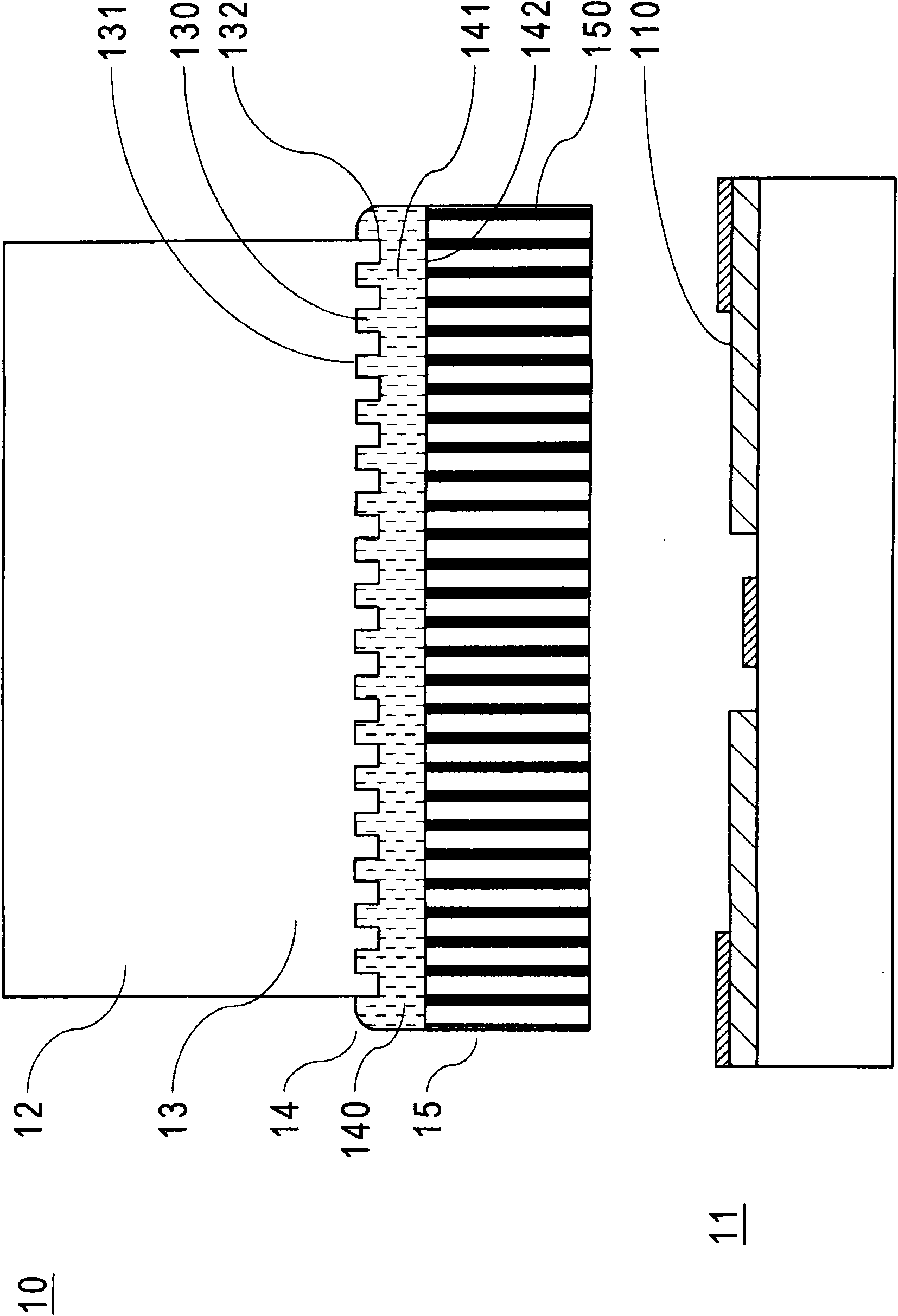
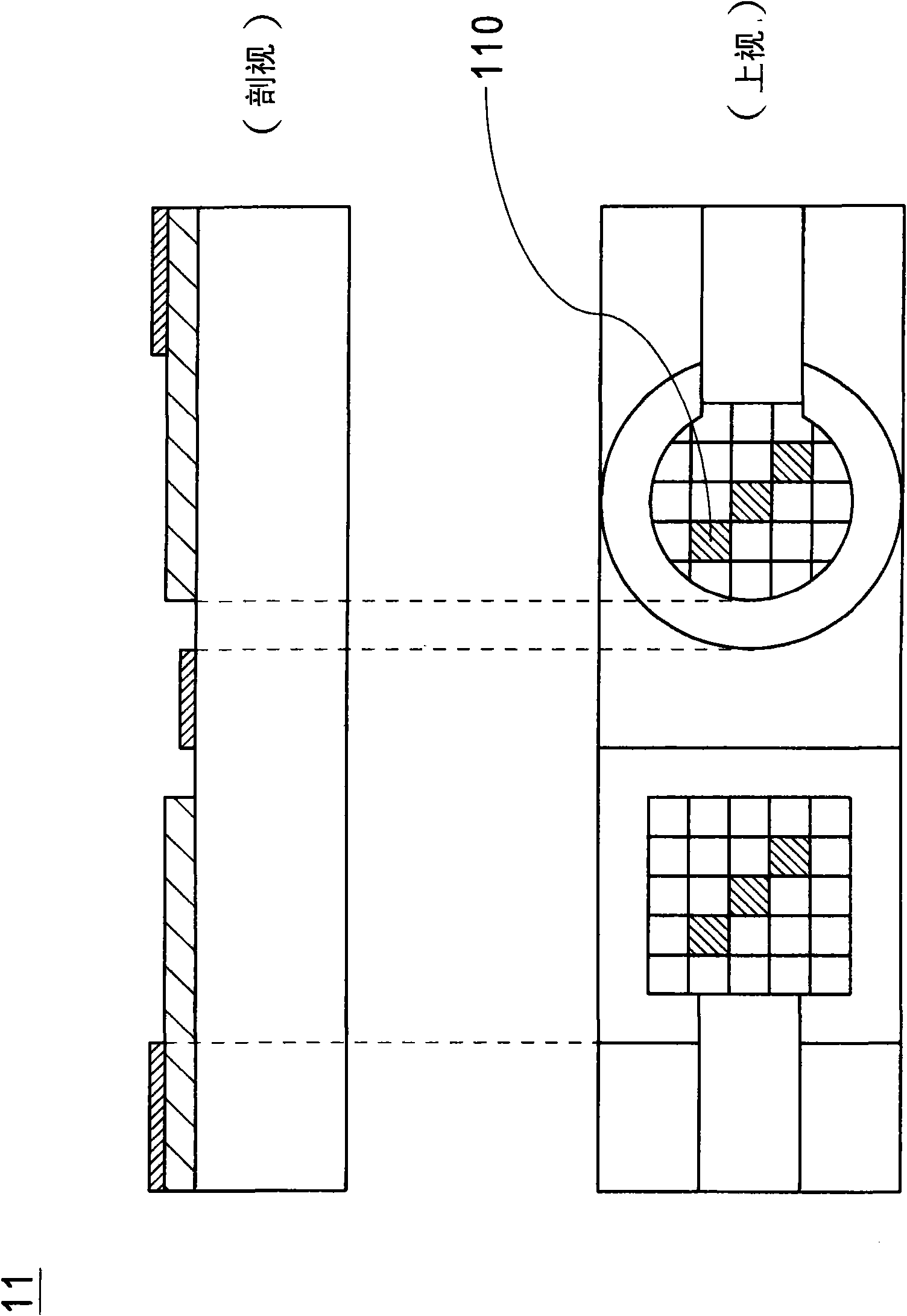
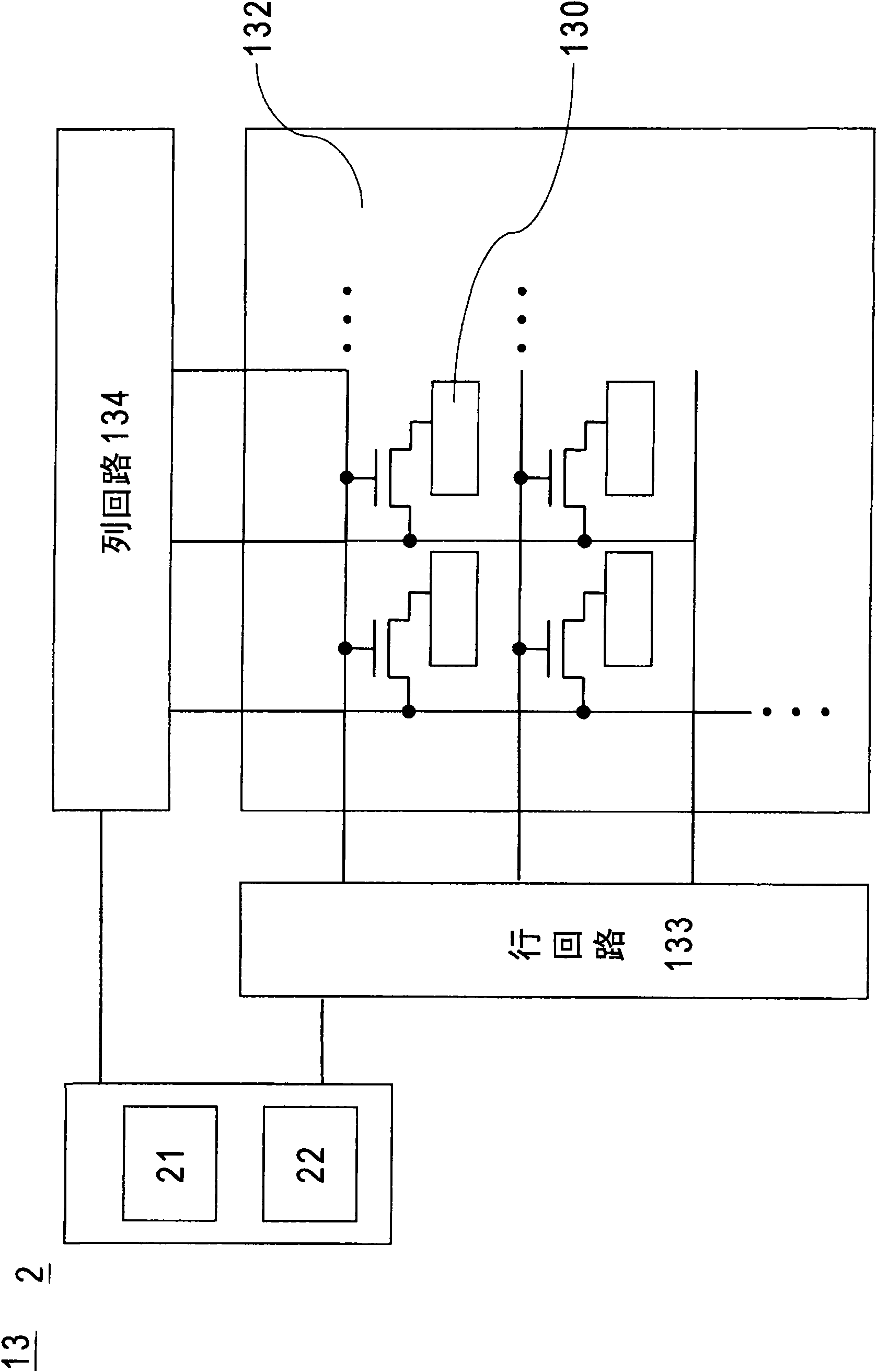
[0022] First please refer to figure 1 , is the first preferred embodiment proposed according to the present invention, which is a cross-sectional structure of an electrical measurement point pixel division test device 10, used to test at least one electrical component 11, wherein the electrical component 11 has a plurality of electrical measurement points 110, such as figure 2 A top view of the electrical component 11 shown. The electrical component 11 may be a printed circuit board or an integrated circuit (IC), such as BGA, QFP, and the like. back to figure 1 The pixel division test device 10 for electrical measurement points mainly includes a glass substrate 12 , a conductive layer 13 , a resin conductive film 14 and a rubber conductive film 15 . The conductive layer 13 includes an upper surface 131 and a lower surface 132 , and the upper surface 131 of the conductive layer 13 is attached to the glass substrate 12 . Additionally, please refer to image 3 , the conduct...


PUM


Abstract

The invention provides a separation testing method of a pixel of an electric testing point and a testing device thereof. The separation testing method of the pixel of the electric testing point comprises the steps of: providing a testing plate which comprises a conductive layer and a glass base plate; operating a row loop and a line loop for controlling the electric conductivity of a pixel contact of the conductive layer; providing at least one electric element; forming a first circuit layout by the electric testing point of the electric element; forming a preset gap between the electric testing point of the electric element and the pixel contact of the testing plate; providing a control module for operating the row loop and the line loop of the conductive layer; enabling the pixel contact to form a second circuit layout; providing an alignment procedure; enabling the second circuit layout to correspond to the first circuit layout; and operating a testing procedure for testing the first circuit layout.

Description

technical field [0001] The present invention relates to a test device and a test method, in particular to a test device and a test method applied to semiconductor elements or printed circuit boards. Background technique [0002] In the past, in the process of testing related electrical components such as printed circuit boards or semiconductor components, different electrical components have different electrical measuring points with different circuit layouts, so test fixtures often need to be replaced with different circuit layouts or electrical measuring points. Or adjust the position and spacing of the probes in the test fixture, so that the probes of the test fixture can be accurately aligned to the electrical measuring points of the electrical components, so as to facilitate the subsequent testing of the electrical components. However, the above-mentioned processing method is time-consuming and greatly affects the test cost. Therefore, how to improve the structure and t...

Claims


Application Information

Patent Timeline
Patent Type & Authority Applications(China)
IPC IPC(8): G01R31/28G01R31/27G01R31/00H01L23/48
Inventor 汪雨萍
Owner 吕佳玲
Why Eureka
Try Eureka