Method for preventing gap below side wall barrier layer during self-aligning silicide process

A self-aligned silicide, barrier layer technology, applied in electrical components, semiconductor/solid-state device manufacturing, circuits, etc., can solve problems such as device leakage, and achieve the effect of preventing gaps

Inactive Publication Date: 2010-09-08
SEMICON MFG INT (SHANGHAI) CORP
View PDF0 Cites 6 Cited by
  • Summary
  • Abstract
  • Description
  • Claims
  • Application Information

AI Technical Summary

Problems solved by technology

As the feature size of the device is reduced so that the distance between the contact layer and the gate of the upper metal interconnection layer is only 60 nanometers, the metal

Method used


Image

  • Method for preventing gap below side wall barrier layer during self-aligning silicide process
  • Method for preventing gap below side wall barrier layer during self-aligning silicide process
  • Method for preventing gap below side wall barrier layer during self-aligning silicide process

Examples


Embodiment Construction

[0053] In order to make the object, technical solution and advantages of the present invention clearer, the present invention will be further described in detail below with reference to the accompanying drawings and examples.

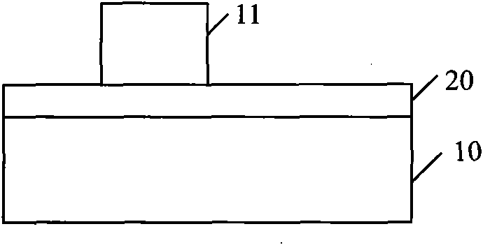
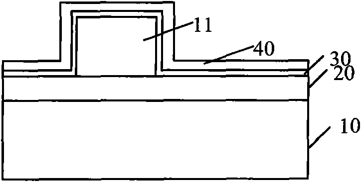
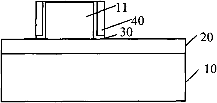
[0054] From figure 2 It can be seen that when the barrier layer of the sidewall of the gate is manufactured by the salicide method, the reason for the gap between the barrier layer, that is, the barrier layer and the device substrate, is: the etching on the device substrate When silicon oxide is used, wet etching is used and due to the relatively thick oxide layer (greater than or equal to 200 angstroms) on the device substrate, the amount of wet etching used is relatively large, resulting in a gap between the barrier layer and the device substrate. The silicon oxide layer is also etched away laterally. Therefore, in order to overcome this defect, the method provided by the present invention first constructs TEOS on the sidewall of the gate to remove ...


PUM

PropertyMeasurementUnit
Thicknessaaaaaaaaaa
Thicknessaaaaaaaaaa
Thicknessaaaaaaaaaa

Abstract

The invention discloses a method for a part to prevent a gap below a side wall barrier layer during a self-aligning silicide process. The part comprises a bedding oxidation film which covers a part underlayer and a grid which is formed on the bedding oxidation film. The method comprises the following steps that: after a sacrificial layer TEOS is deposited, the sacrificial layer and the bedding oxidation film covering the part underlayer are etched until the surface of the part underalyer and the grid top part; and during the manufacturing process of the side wall barrier layer of the grid, by utilizing the self-aligning silicide way, the thickness of the oxidation layer which is deposited on the part underlayer which is etched in a wet way is more than or equal to 100 angstroms and is less than 200 angstroms. The method can prevent the gap below the barrier layer during the self-aligning process of silicide.

Description

technical field [0001] The invention relates to semiconductor device manufacturing technology, in particular to a method for preventing gaps under barrier layers in the process of self-aligned silicide. Background technique [0002] In the manufacturing process of integrated circuits, the device needs to be metallized. Metallization is the process of depositing a metal film on an insulating dielectric film and then marking a pattern in the device manufacturing process to form interconnection metal lines and hole filling plugs for devices. For example, a metal interconnection layer is deposited on the active area (AA, Active Region) of the device. [0003] With the performance optimization of the integrated circuit, the feature size of the device is further reduced, and the cross-section of the electrical contact between the AA and the metal interconnection layer is very small, and this small electrical contact surface will lead to an increase in the contact resistance. In o...

Claims


Application Information

Patent Timeline
IPC IPC(8): H01L21/336
Inventor 叶兰御周儒领黄淇生詹奕鹏
Owner SEMICON MFG INT (SHANGHAI) CORP
Why Eureka
Try Eureka