Silicon controlled rectifier electrostatic discharge protection circuit structure triggered by grid controlled diode

A gate-controlled diode and electrostatic discharge technology, applied in the electronic field, can solve problems such as unfavorable internal circuit device protection, and achieve the effect of low trigger voltage

Inactive Publication Date: 2010-09-08
UNIV OF ELECTRONICS SCI & TECH OF CHINA
View PDF3 Cites 20 Cited by
  • Summary
  • Abstract
  • Description
  • Claims
  • Application Information

AI Technical Summary

Problems solved by technology

for figure 1 For the SCR structure shown, to increase its sustain voltage, it is necessary to increase the P well package cathode N + or N well package anode P + The distance, and the increase of these two size parameters will often bring higher device trigger voltage, which is not conducive to the device protection of the internal circuit

Method used


Image

  • Silicon controlled rectifier electrostatic discharge protection circuit structure triggered by grid controlled diode
  • Silicon controlled rectifier electrostatic discharge protection circuit structure triggered by grid controlled diode
  • Silicon controlled rectifier electrostatic discharge protection circuit structure triggered by grid controlled diode

Examples


specific Embodiment approach 1

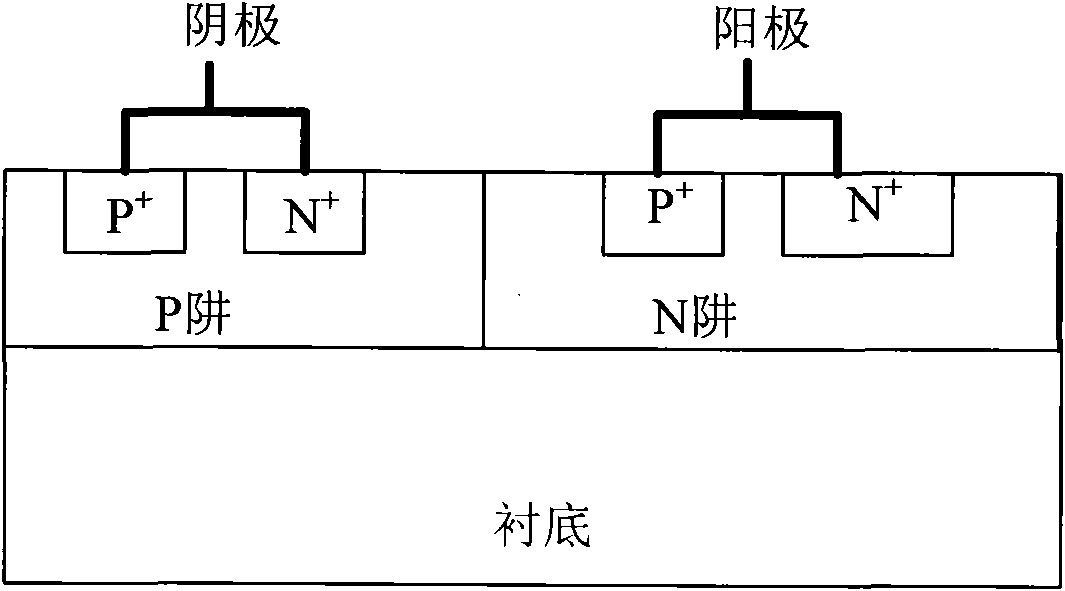
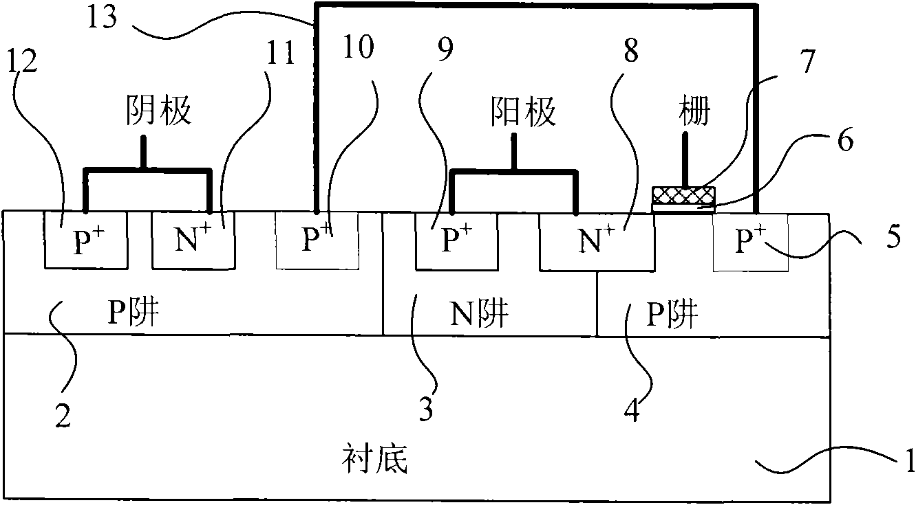
[0021] A thyristor rectifier type electrostatic discharge protection circuit structure triggered by a gate control diode, such as image 3 As shown, it includes: two conductive types of well regions located on a semiconductor substrate substrate 1: a P-type well region 2 and an N-type well region 3; two heavily doped regions located in the first P-type well region 2 District: P + Heavily doped region 12 and N + Heavily doped region 11; two heavily doped regions located in the N-type well region 3: P + Heavily doped region 9 and N + Heavily doped region 8; a first electrode that contacts the surface of the two heavily doped regions in the first P-type well region 2; a second electrode that contacts the surface of the two heavily doped regions in the N-type well region 3 . The protection circuit structure also includes a second P-type well region 4, which is connected to the first P-type well region 2 and surrounds the N-type well region 3 in the middle, and the N-type well region...

specific Embodiment approach 2

[0028] A gate-controlled diode-triggered silicon controlled rectifier type electrostatic discharge protection circuit structure, comprising: two conductive types of well regions on a semiconductor substrate substrate 1: N-type well region 2 and P-type well region 3; Two heavily doped regions in the first N-type well region 2: N + Heavily doped region 12 and P + Heavily doped region 11; two heavily doped regions located in the P-type well region 3: N + Heavily doped region 9 and P + Heavily doped region 8; a first electrode in surface contact with the two heavily doped regions in the first N-type well region 2; a second electrode in surface contact with the two heavily doped regions in the P-type well region 3 . The protection circuit structure further includes a second N-type well region 4, the second N-type well region 4 is connected to the first N-type well region 2 and surrounds the P-type well region 3 in the middle, and the P-type well region P in zone 3 + A part of the he...


PUM


Abstract

The invention relates to a silicon controlled rectifier (SCR) electrostatic discharge (ESD) protection circuit structure triggered by a grid controlled diode, belonging to the technical field of electronics. Through integrating the grid controlled diode with low breakdown voltage, the trigger voltage of a conventional SCR ESD protection circuit structure is converted to the breakdown voltage of a grid controlled N+/P well (or N well/P+) node from the breakdown voltage of a P well/N well node, thereby reducing the trigger voltage of the SCR ESD and finally well protecting a circuit in a chip. Moreover, through changing the grid controlled bias voltage of the grid controlled diode, the trigger voltage of the SCR ESD protection circuit structure can be controlled; and through simply adjusting the dimension parameters of a device, the controllable maintaining voltage of the device can be obtained. The structure is suitable for technologies such as CMOS, BiMOS, BCD, SOI and the like, can be connected between an integrated circuit and a power supply and is used as the ESD protection of a power clamp, and can also be connected between the input port and the output port of the integrated circuit and the power supply (ground) and is used as the ESD protection of the input port and the output port.

Description

Technical field [0001] The present invention belongs to the field of electronic technology, and relates to a protection circuit used for electrostatic discharge (ESD) in an integrated circuit, and more particularly to a silicon controlled rectifier (Semiconductor Controlled Rectifier, SCR) electrostatic discharge circuit structure. Background technique [0002] Electrostatic discharge is a common phenomenon in the manufacturing, production, assembly, testing, storage, and handling of semiconductor devices or circuits. The excess charge it brings will pass through the IC of the integrated circuit in a very short time. The / O pin passes into the integrated circuit and destroys the internal circuit of the integrated circuit. To solve this problem, manufacturers usually install a protection circuit between the internal circuit and the I / O pins. The protection circuit must be activated before the pulse current of electrostatic discharge reaches the internal circuit to quickly eliminat...

Claims


Application Information

Patent Timeline
Patent Type & Authority Applications(China)
IPC IPC(8): H01L27/07H01L29/06
Inventor 蒋苓利樊航张波乔明林丽娟喻钊钟昌贤
Owner UNIV OF ELECTRONICS SCI & TECH OF CHINA
Why Eureka
Try Eureka