Method for enhancing pressure resistance capacity of chip in packaging process and chip thereof

A technology for compressive strength and chip enhancement, which is applied in the manufacture of electrical components, electrical solid devices, semiconductor/solid state devices, etc. It can solve problems such as poor compressive capacity, collapse of insulating dielectric layers, scrapped chips, etc., to improve reliability, The effect of preventing capacitance and enhancing the ability to resist pressure

Active Publication Date: 2010-09-15
SHANGHAI HUAHONG GRACE SEMICON MFG CORP
View PDF4 Cites 5 Cited by
  • Summary
  • Abstract
  • Description
  • Claims
  • Application Information

AI Technical Summary

Problems solved by technology

There are voids in the metal interlayer insulating layer IMD and the insulating dielectric layer formed by the deposition of amorphous materials. Therefore, such intermetal insulating layer IMD and insulating dielectric layer are very fragile and have poor pressure resistance. chippackage) when bonding wires, the fragile metal interlayer insulating layer IMD and insulating dielectric layer are easy to collapse under pressure, so that the chip is scrapped

Method used


Image

  • Method for enhancing pressure resistance capacity of chip in packaging process and chip thereof
  • Method for enhancing pressure resistance capacity of chip in packaging process and chip thereof
  • Method for enhancing pressure resistance capacity of chip in packaging process and chip thereof

Examples


Embodiment Construction

[0033] The following will combine Figure 2A ~ Figure 2I A further detailed description will be made on the method of the present invention for enhancing the pressure resistance capability of chip packaging and the chip thereof.

[0034] The method of the present invention to enhance the pressure resistance capability of chip packaging is to add a pattern for forming a through hole in the redundant area of ​​each metal interlayer insulating layer mask and the redundant area of ​​each metal interconnection mask. The pattern added in the redundant area of ​​the n metal interconnection reticle corresponds to the pattern added in the redundant area of ​​the nth metal interlayer insulating layer reticle, and the redundancy of the n+1 metal interlayer insulating layer reticle The pattern added in the region corresponds to the pattern added in the redundant region of the nth metal interconnection mask, where n=1, 2, 3, . . . , N.

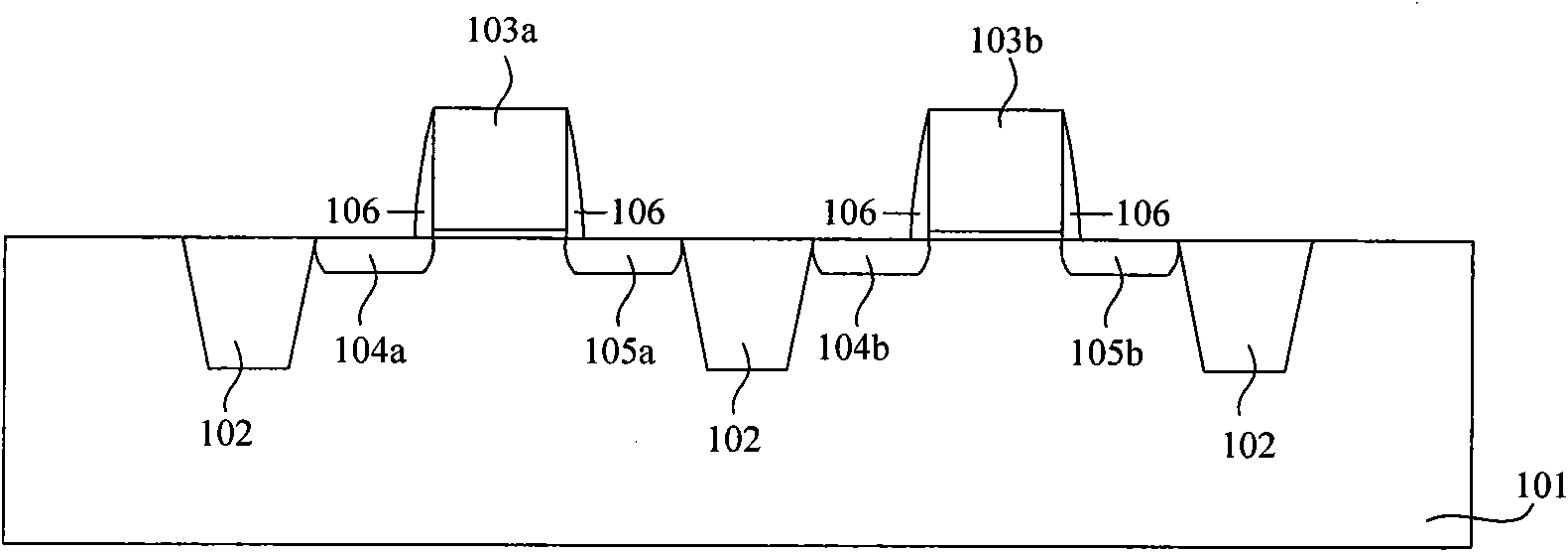
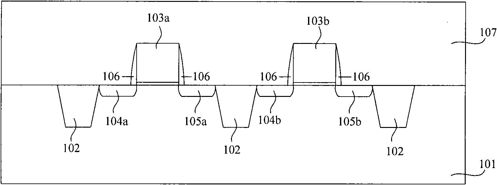
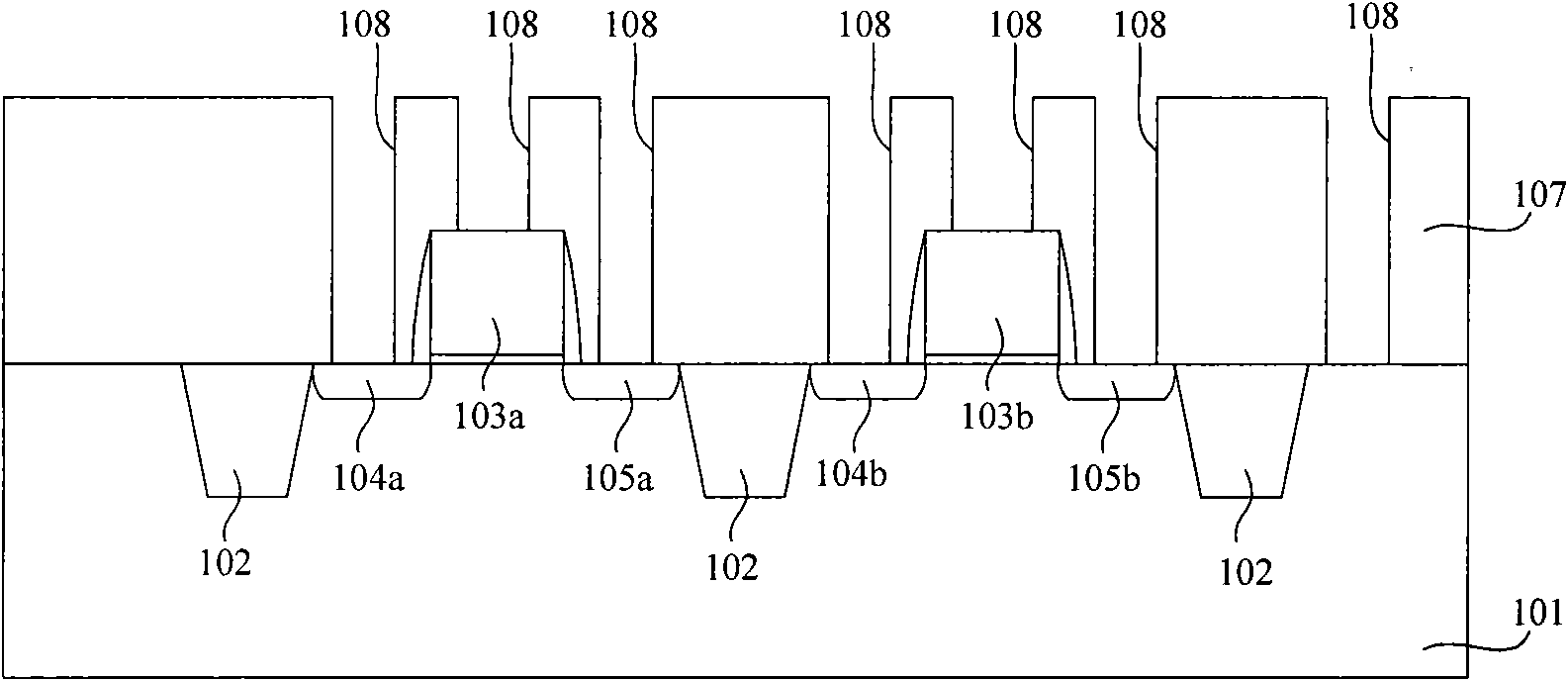
[0035] see Figure 2I The chip of the present inve...


PUM


Abstract

The invention relates to a method for enhancing the pressure resistance capacity of a chip in the packaging process and the chip thereof. The method comprises the following steps of: additionally arranging patterns used for forming through holes in a redundancy region of each metal interlayer insulation layer mask and a redundancy region of each metal interconnect mask, wherein the pattern additionally arranged in the redundancy region at the nth metal interconnect mask corresponds to the pattern additionally arranged in the redundancy region of the nth metal interlayer insulation layer mask, and the pattern additionally arranged in the redundancy region of the (n+1)th metal interlayer insulation layer mask corresponds to the pattern additionally arranged in the redundancy region of the nth metal interconnect mask, wherein n is 1, 2, 3 till N. The method for enhancing the pressure resistance capacity of the chip in the packaging process and the chip thereof can improve the pressure resistance capacity of the chip, thereby improving the manufacturing reliability of the chip.

Description

technical field [0001] The invention relates to semiconductor manufacturing technology, in particular to a method for enhancing the pressure resistance capability of chip packaging and the chip thereof. Background technique [0002] The following briefly introduces the manufacturing process of semiconductor devices below 65nm: [0003] Such as Figure 1A As shown, an active region and an isolation trench 102 separating the active region are formed on the substrate 101. The active region includes a gate formed on the surface of the substrate 101 and a gate formed under the surface of the substrate 101. . The source region and the drain region on both sides of the gate, the isolation groove 102 is located below the surface of the substrate 101, and sidewalls 106 are formed on both sides of the gate; [0004] exist Figure 1A Among them, the gate 103a, the source region 104a and the drain region 105a form a P-type field effect transistor, and the gate 103b, the source region 1...

Claims


Application Information

Patent Timeline
Patent Type & Authority Applications(China)
IPC IPC(8): H01L21/60H01L23/485
Inventor 雷强刘正超沈亮
Owner SHANGHAI HUAHONG GRACE SEMICON MFG CORP
Why Eureka
Try Eureka