

Improved method for semi-conductor flip-chip bonding package cooling
A technology of flip-chip packaging and manufacturing method, which is applied in the direction of semiconductor/solid-state device manufacturing, semiconductor device, semiconductor/solid-state device components, etc. , the heat dissipation effect is not obvious and other problems, it is beneficial to achieve the stress absorption function, meet the ultra-high heat dissipation requirements, and improve the electrothermal performance and reliability.
- Summary
- Abstract
- Description
- Claims
- Application Information
AI Technical Summary
Problems solved by technology
Method used
Image

Examples
Embodiment Construction
[0039] Below in conjunction with specific embodiment, further illustrate the present invention. It should be understood that these examples are only used to illustrate the present invention and are not intended to limit the scope of the present invention. In addition, it should be understood that after reading the teachings of the present invention, those skilled in the art can make various changes or modifications to the present invention, and these equivalent forms also fall within the scope defined by the appended claims of the present application.
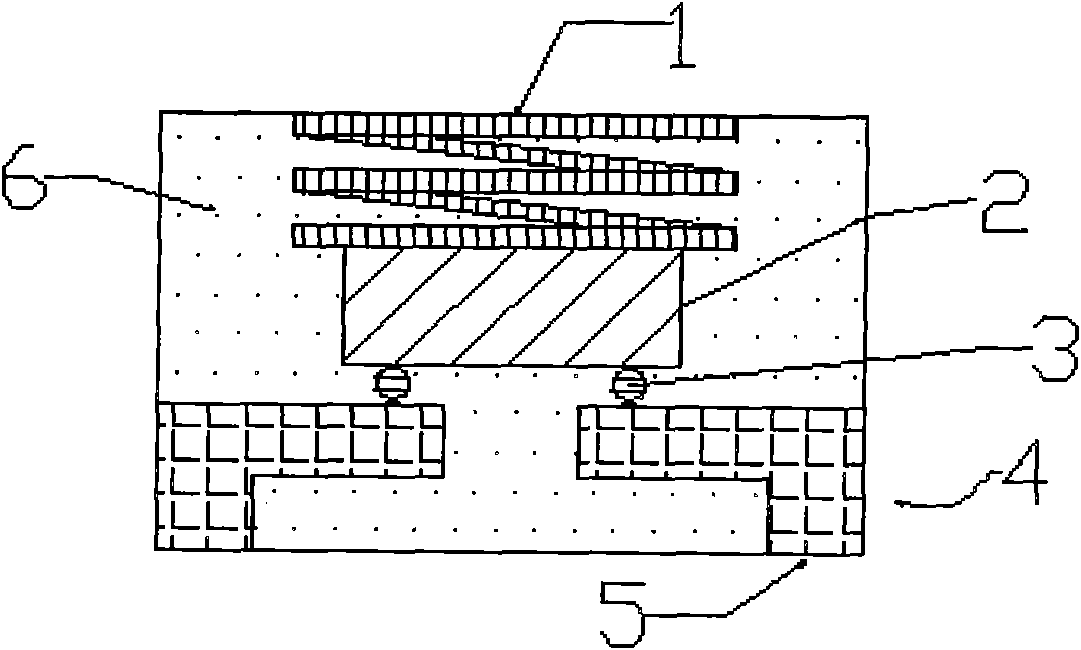
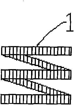
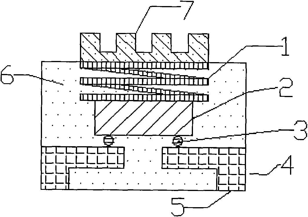
[0040] Embodiments of the present invention relate to a method for improving heat dissipation of semiconductor flip-chip packaging. According to the method, such as figure 1 The package structure shown includes a chip 2, an electrical interconnection material 3, a lead frame 4 and a molding compound 6, and the package heat dissipation improvement structure also includes a spring radiator 1; the lead frame 4 is provided with a t...
PUM
 Abstract
Description
Claims
Application Information