Supercharge Your Innovation With Domain-Expert AI Agents!

LED device

A technology of LED devices and LED chips, applied in the direction of electric solid-state devices, semiconductor devices, electrical components, etc., can solve problems affecting the reliability of LED chip circuit connections, affecting the light output efficiency of LED chips, unfavorable chip installation and integration, etc., to achieve Conducive to integration, simple structure, and reduced thickness

Inactive Publication Date: 2010-10-13
广州市海林电子科技发展有限公司
View PDF6 Cites 6 Cited by
  • Summary
  • Abstract
  • Description
  • Claims
  • Application Information

AI Technical Summary

Problems solved by technology

[0004] 1. Due to the gull-wing structure of gold wire bending, the thickness of the LED chip after packaging is thicker, which is not conducive to the installation and integration of the chip;
[0005] 2. Since the gold wire is thinner, the current passing through the LED chip is smaller under the same voltage, which will affect the light output efficiency of the LED chip;
[0006] 3. Due to the poor thermal conductivity of the thin gold wire, it is not conducive to the heat dissipation of the LED chip;
[0007] 4. Since the LED chip is electrically connected to the external circuit after being bent by the gold wire, the gold wire may break during transportation or circuit connection extrusion, which will affect the reliability of the circuit connection after the LED chip is packaged

Method used


Image

  • LED device
  • LED device
  • LED device

Examples


Embodiment Construction

[0025] In order to make the present invention easier to understand, the present invention will be further described below in conjunction with the drawings, but the embodiments in the drawings do not constitute any limitation to the present invention.

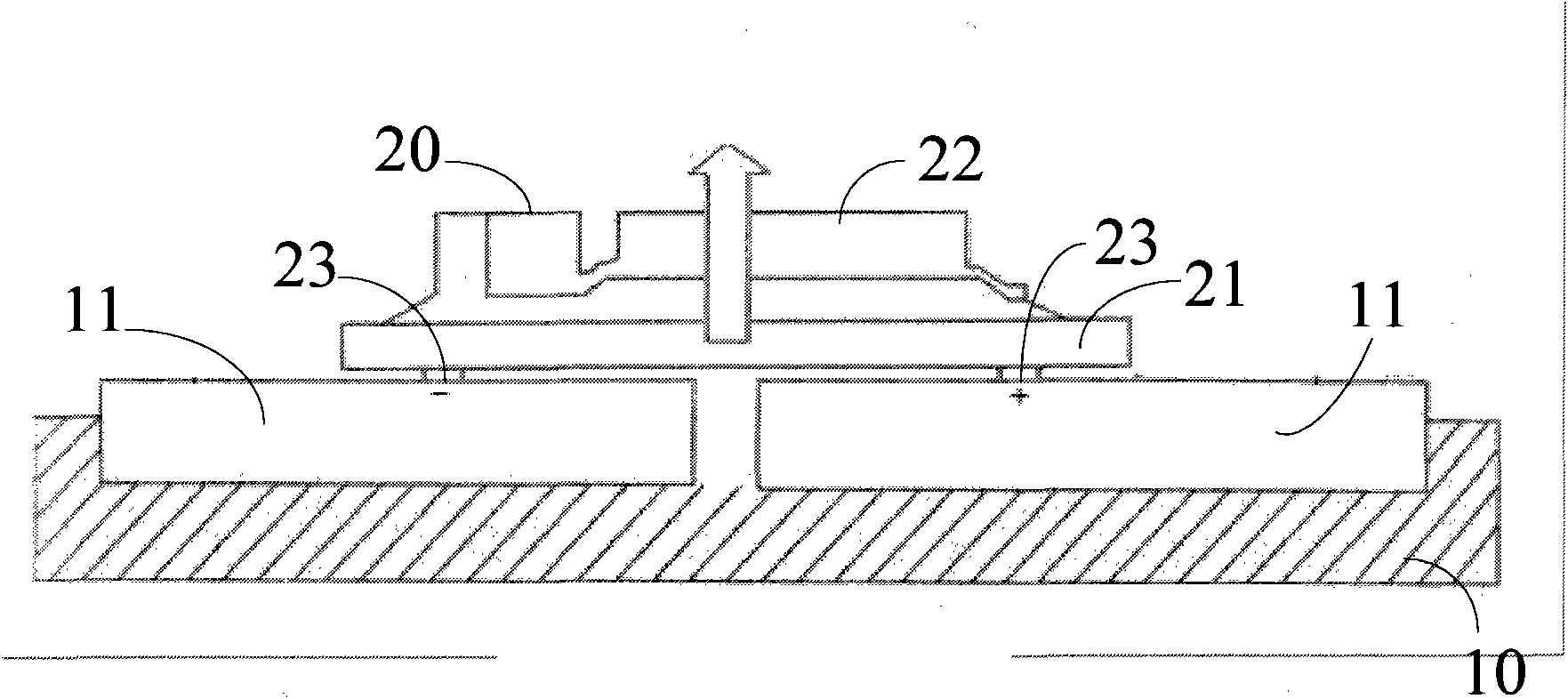
[0026] A kind of LED device of the present invention, as figure 1 with figure 2 As shown, it includes a substrate 10 with a printed circuit, an LED chip 20, the LED chip 20 includes a substrate 21, a light emitting part 22, a light conversion part (not shown in the figure), etc., the substrate 10 has a heat dissipation function, The two poles 23 of the LED chip 20 are arranged on the back of the substrate 21 , and the two poles 23 of the LED chip 20 are mounted on the pads 11 of the substrate 10 , so as to realize the connection between the LED chip 20 and the external circuit.

[0027] Preferably, the substrate 10 of the embodiment of the present invention adopts an aluminum substrate 10 because the aluminum substrate 10 has ...


PUM


Abstract

The invention discloses an LED device, which comprises a substrate and an LED chip, wherein the LED chip comprises a substrate and a luminous part; two poles of the LED chip are arranged on the back of the substrate; and the two poles of the LED chip are jointed on a pad of the substrate. The LED device has the advantages of simple structure, convenient installation, thin thickness after encapsulation, high light emitting efficiency, good luminous effect, good heat dissipation performance, high reliability and long service life.

Description

technical field [0001] The invention relates to a semiconductor packaging structure, in particular to an LED device. Background technique [0002] The existing LED device is to fix the LED chip on the substrate, wherein the LED chip includes a light-emitting part and a bottom substrate, the two poles of the LED chip are located above the LED chip, and the LED chip is bent by the gold wire extending from the two poles of the LED chip. After that, it is electrically connected to the pad of the substrate. [0003] However, the way in which the LED chip of the prior art is connected to the substrate after bending the gold wire has the following disadvantages: [0004] 1. Due to the gull-wing structure of gold wire bending, the thickness of the LED chip after packaging is thicker, which is not conducive to the installation and integration of the chip; [0005] 2. Since the gold wire is thinner, the current passing through the LED chip is smaller under the same voltage, which wi...

Claims


Application Information

Patent Timeline
Patent Type & Authority Applications(China)
IPC IPC(8): H01L33/36H01L33/62H01L25/075
Inventor 邢瑞林汤丹周宏英曾剑
Owner 广州市海林电子科技发展有限公司
Features
  • R&D
  • Intellectual Property
  • Life Sciences
  • Materials
  • Tech Scout
  • Unparalleled Data Quality
  • Higher Quality Content
  • 60% Fewer Hallucinations
Learn More