Semiconductor device

一种半导体、氧化物半导体的技术,应用在半导体激光器、半导体激光器的结构细节、激光器等方向,达到改善粘合、接触面积增加的效果

Inactive Publication Date: 2010-10-20
SONY CORP
View PDF2 Cites 5 Cited by
  • Summary
  • Abstract
  • Description
  • Claims
  • Application Information

AI Technical Summary

Problems solved by technology

However, parasitic capacitance is generated between the electrode pad and the lower DBR layer

Method used


Image

  • Semiconductor device
  • Semiconductor device
  • Semiconductor device

Examples


Embodiment Construction

[0020] Hereinafter, modes for carrying out the present invention will be described in detail with reference to the accompanying drawings. Description will be made in the following order.

[0021] 1. Structure

[0022] 2. Manufacturing method

[0023] 3. Function and effect

[0024] 4. Modify

[0025] structure

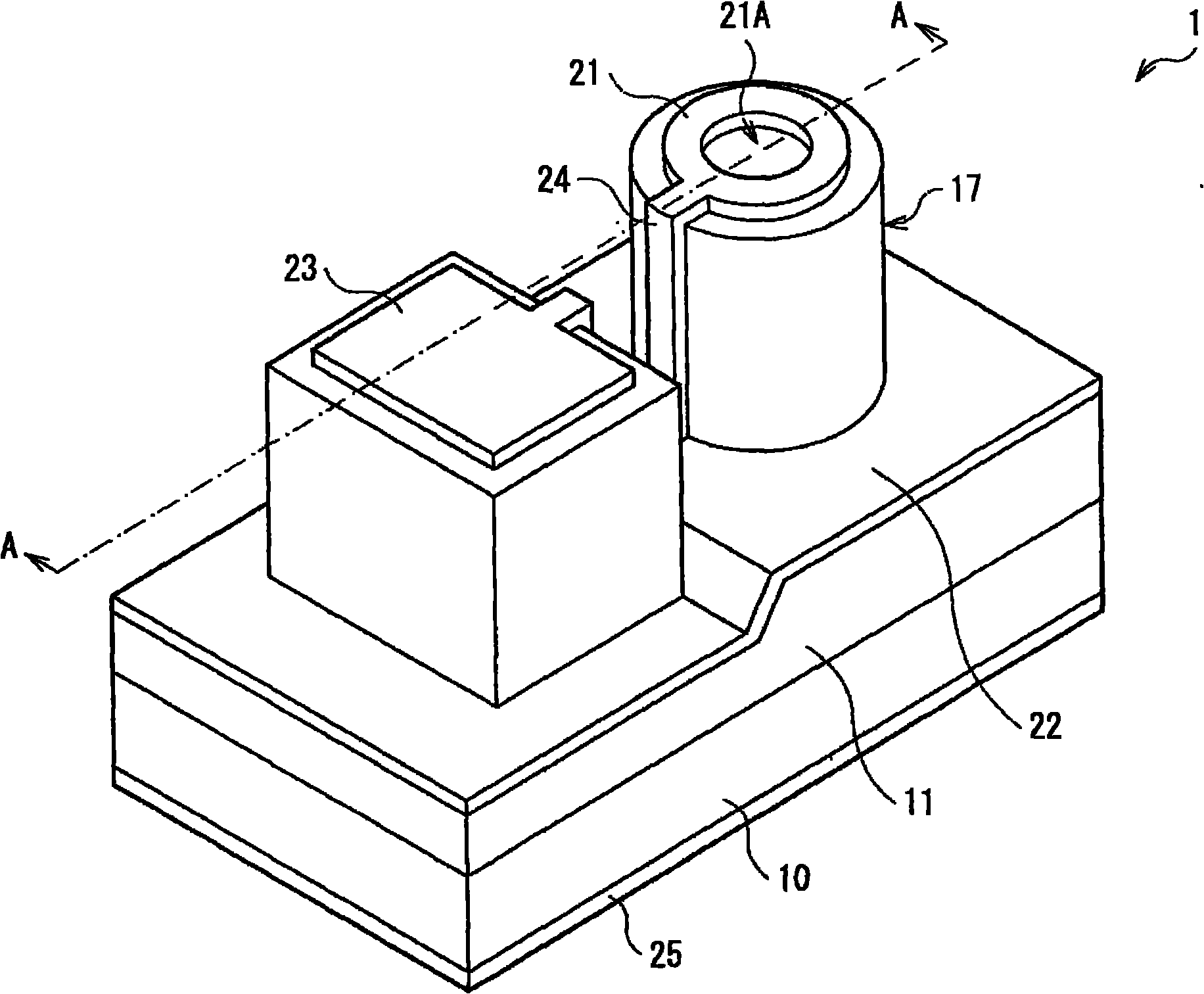
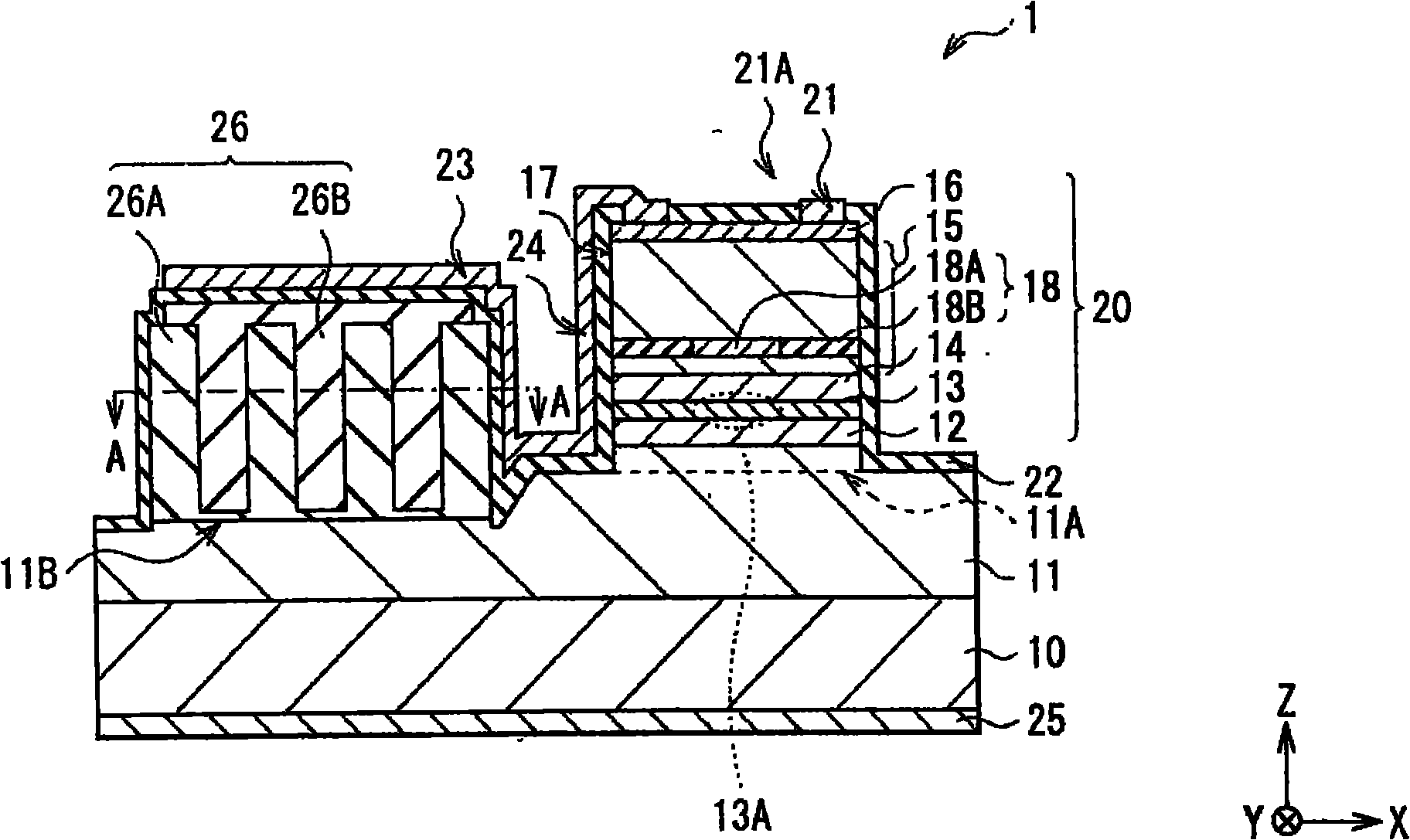
[0026] figure 1 is a perspective view of a vertical cavity surface emitting laser diode 1 according to an embodiment of the present invention. figure 2 Illustrated figure 1 An example of a cross-sectional configuration of the laser diode 1 taken along line A-A. figure 1 and 2 is a schematic, and figure 1 and 2 The size and shape in may differ from the actual product.

[0027] The laser diode 1 of this embodiment has a stack structure 20 in which a lower DBR layer 11, a lower spacer layer 12, an active layer 13, an upper spacer layer 14, an upper DBR layer 15, and a contact layer 16 are sequentially stacked on one surface side of a substrate 10 superior. I...


PUM


Abstract

The present invention provides a semiconductor device realizing improved adhesion between a low-dielectric-constant material and a semiconductor material. The semiconductor device includes, on a semiconductor layer, an adhesion layer and a low-dielectric-constant material layer in order from the semiconductor layer side. The adhesion layer has a projection / recess structure, and the low-dielectric-constant material layer is formed so as to bury gaps in the projection / recess structure.

Description

technical field [0001] The present invention relates to a semiconductor device having improved adhesion between a low dielectric constant material and a semiconductor. Background technique [0002] Vertical-cavity surface-emitting lasers (VCSELs) consume less power than edge-emitting laser diodes, and VCSELs can be directly modulated. Therefore, VCSELs have been used as inexpensive light sources for optical communications in recent years. [0003] A VCSEL generally has a cylindrical mesa in which a lower distributed Bragg reflection (DBR) layer, a lower spacer layer, an active layer, an upper spacer layer, an upper DBR layer, and a contact layer are sequentially stacked on a substrate. The lower DBR layer or the upper DBR layer is provided with a current narrowing layer having a structure of narrowing a current injection region in order to increase the efficiency of injecting current to the active layer and reduce a threshold current. Electrodes are provided for both the t...

Claims


Application Information

Patent Timeline
Patent Type & Authority Applications(China)
IPC IPC(8): H01S5/183H01S5/02
CPCH01S5/0425H01S5/1835H01S5/02276H01S5/34313H01S2301/176H01S5/18311B82Y20/00H01S5/06226H01S5/04256H01S5/02345
Inventor 增井勇志荒木田孝博菊地加代子成瀬晃和大木智之城岸直辉
Owner SONY CORP
Why Eureka
Try Eureka