Method and system for optoelectronics transceivers integrated on a CMOS chip

A photoelectric detector and chip technology, applied in electromagnetic transceivers, instruments, optics, etc., can solve problems such as high power, complexity and cable volume cost

Inactive Publication Date: 2010-10-20
LUXTERA
View PDF8 Cites 14 Cited by
  • Summary
  • Abstract
  • Description
  • Claims
  • Application Information

AI Technical Summary

Problems solved by technology

It can be mitigated to some extent by equalization, decoding, and shielding, but these techniques require considerable power, complexity, and cable volume penalties while providing only mediocre achievable improvements and very limited scalability

Method used


Image

  • Method and system for optoelectronics transceivers integrated on a CMOS chip
  • Method and system for optoelectronics transceivers integrated on a CMOS chip
  • Method and system for optoelectronics transceivers integrated on a CMOS chip

Examples


Embodiment Construction

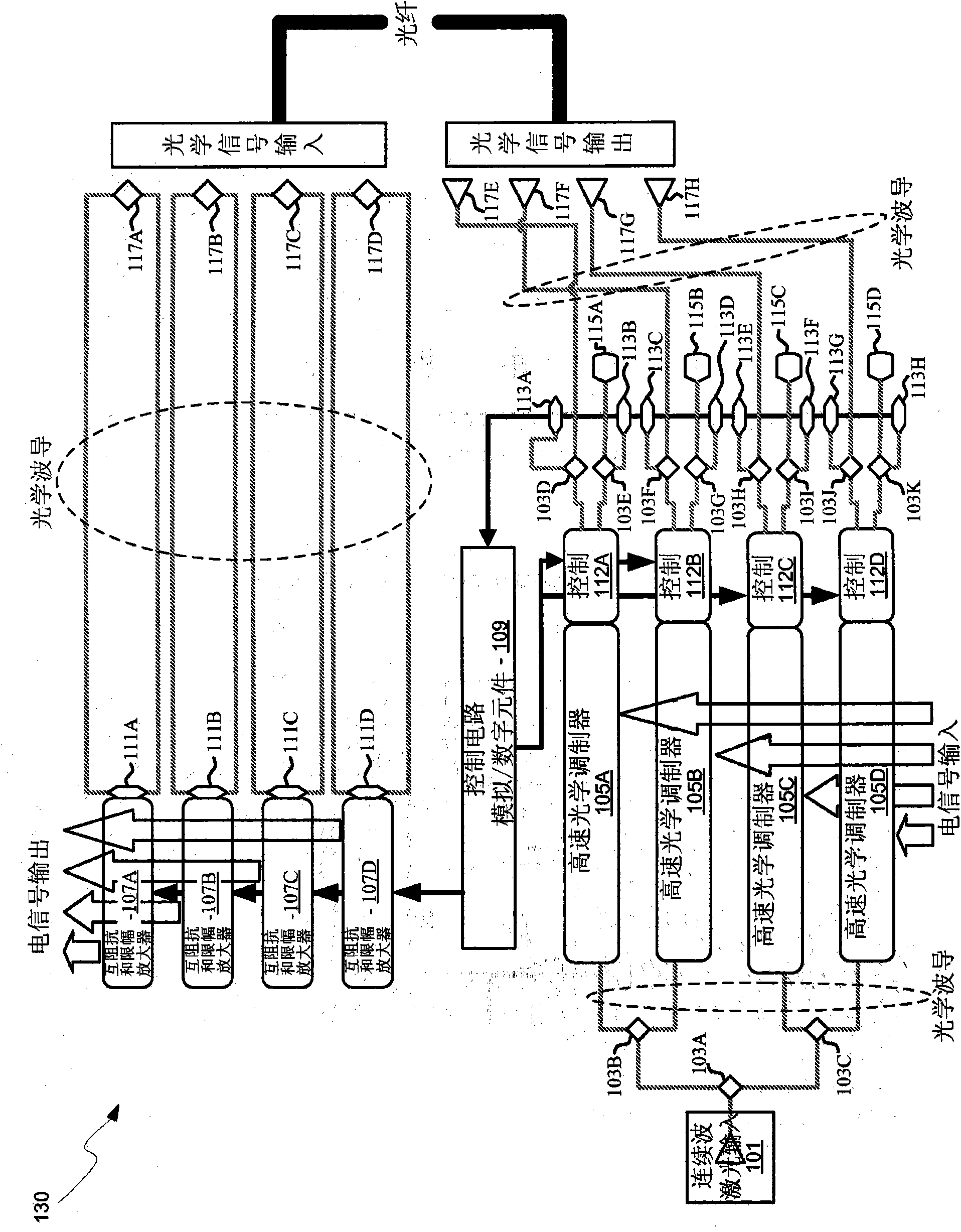
[0027] Certain aspects of the present invention can be found in methods and systems for optoelectronic transceivers integrated on CMOS chips. Exemplary aspects of the invention may include receiving optical signals from one or more optical fibers via a grating coupler on the top surface of the CMOS chip. Optical signals can be converted to electrical signals via one or more photodetectors integrated in or on the CMOS chip. Electrical signals can be processed via circuits in the CMOS chip. A continuous wave (CW) optical signal may be received from a laser source via a grating coupler on the top surface of the CMOS chip and may be modulated via one or more optical modulators integrated in or on the CMOS chip . Electrical signals can be received via circuitry in the CMOS chip and can drive the one or more optical modulators. The modulated optical signal can be transmitted out of the top surface of the CMOS chip into one or more optical fibers via one or more grating couplers i...


PUM


Abstract

Methods and systems for optoelectronics transceivers integrated on a CMOS chip are disclosed and may include receiving optical signals from optical fibers via grating couplers on a top surface of a CMOS chip, which may include a guard ring. Photodetectors may be integrated in the CMOS chip. A CW optical signal may be received from a laser source via grating couplers, and may be modulated using optical modulators, which may be Mach-Zehnder and/or ring modulators. Circuitry in the CMOS chip may drive the optical modulators. The modulated optical signal may be communicated out of the top surface of the CMOS chip into optical fibers via grating couplers. The received optical signals may be communicated between devices via waveguides. The photodetectors may include germanium waveguide photodiodes, avalanche photodiodes, and/or heterojunction diodes. The CW optical signal may be generated using an edge-emitting and/or a vertical-cavity surface emitting semiconductor laser.

Description

[0001] CROSS-REFERENCE / INCORPORATION BY REFERENCE TO RELATED APPLICATIONS [0002] This application references and claims priority to U.S. Provisional Application No. 61 / 057,127, filed May 29, 2008, and U.S. Provisional Application No. 60 / 997,298, filed October 2, 2007, the full text of which Incorporated herein by reference. [0003] This application is also a continuation-in-part of US Patent Application Serial No. 11 / 611,084, filed December 14,2006. [0004] This application also refers to US Patent Nos. 6,895,148, 7,039,258, 7,245,803, and 7,366,380. [0005] Each of the above-mentioned applications and patents is incorporated herein by reference in its entirety. [0006] Federally funded research or development [0007] [Not applicable] [0008] [Microfilm / Copyright Reference] [0009] [Not applicable] technical field [0010] Certain embodiments of the invention relate to integrated circuit power control. More specifically, certain embodiments of the invention re...

Claims


Application Information

Patent Timeline
Patent Type & Authority Applications(China)
IPC IPC(8): G02B6/26
CPCG02B6/124G02B6/30G02B6/4209G02B6/4214H04B10/40
Inventor 蒂埃里·潘盖斯特芬·格勒克纳谢里夫·阿布达拉西纳·米尔赛蒂彼得·德·多伯拉尔
Owner LUXTERA
Why Eureka
Try Eureka