
Black level correction circuit and solid-state imaging device

A black level, correction circuit technology, applied in color TV, color TV parts, TV and other directions, can solve the problem of no digital processing, undisclosed feedback circuit, etc., to ensure the effect of dynamic range

Inactive Publication Date: 2010-10-27
SONY GRP CORP
View PDF9 Cites 2 Cited by
  • Summary
  • Abstract
  • Description
  • Claims
  • Application Information

AI Technical Summary

Problems solved by technology

[0005] In JP-A-2007-059991 (Patent Document 1), an ADC (Analog-Digital Converter) and a DAC (Digital-Analog Converter) in a solid-state imaging device are disclosed, however, use for correcting overdark shading is not disclosed feedback circuit
In JP-A-2006-222708 (Patent Document 2), a correction circuit for over-black shading in a MOS image sensor mounted on a cellular phone is disclosed, but there is nothing about a correction circuit for correcting a black level in a feedback circuit. Description of digital processing and gain switching to adjust the amount of feedback

Method used


Image

  • Black level correction circuit and solid-state imaging device
  • Black level correction circuit and solid-state imaging device
  • Black level correction circuit and solid-state imaging device

Examples


Embodiment Construction

[0023] Hereinafter, the best mode for carrying out the present invention will be explained. Description will be given in the following order.

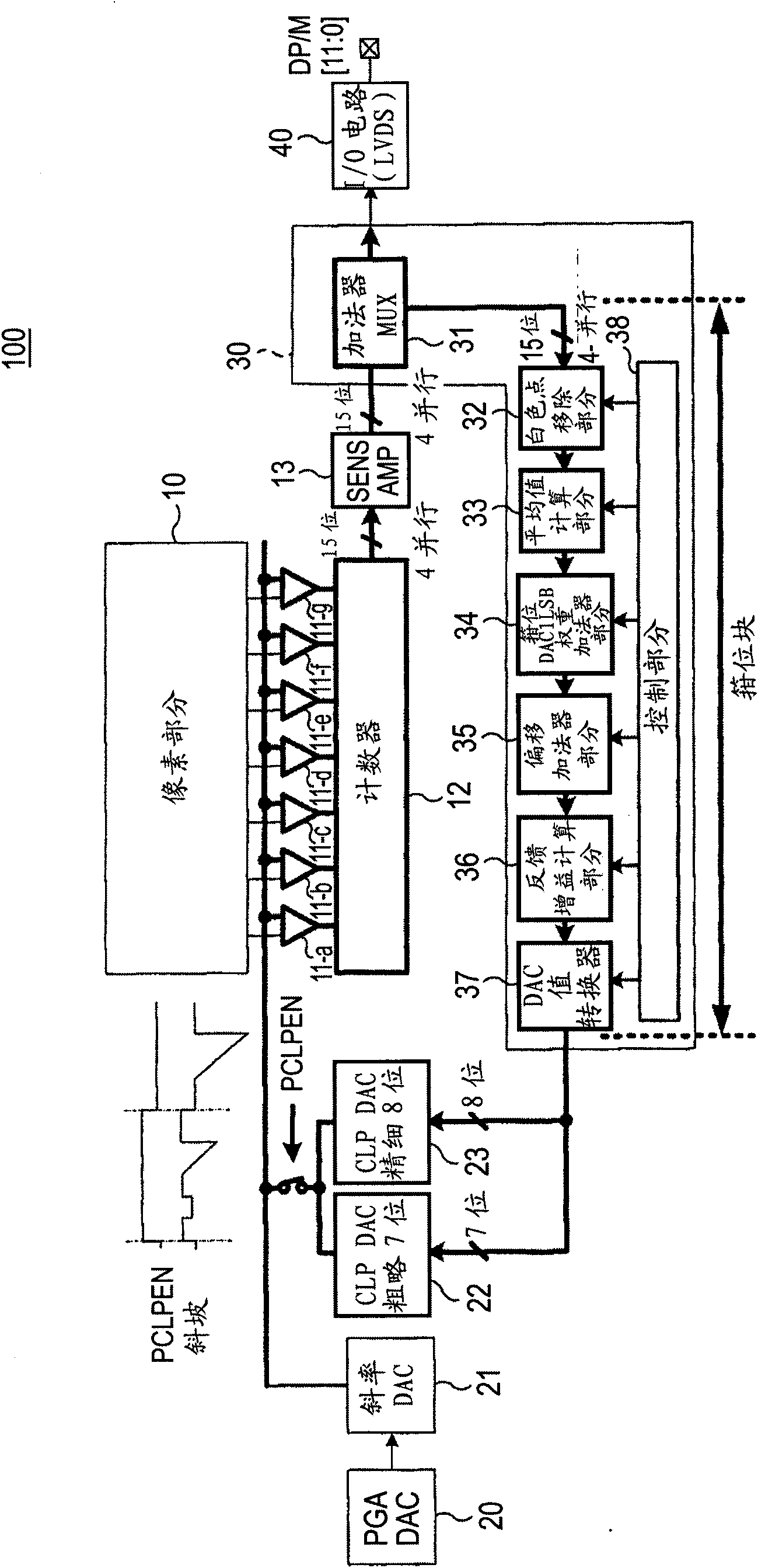
[0024] 1. Block configuration of black level correction circuit

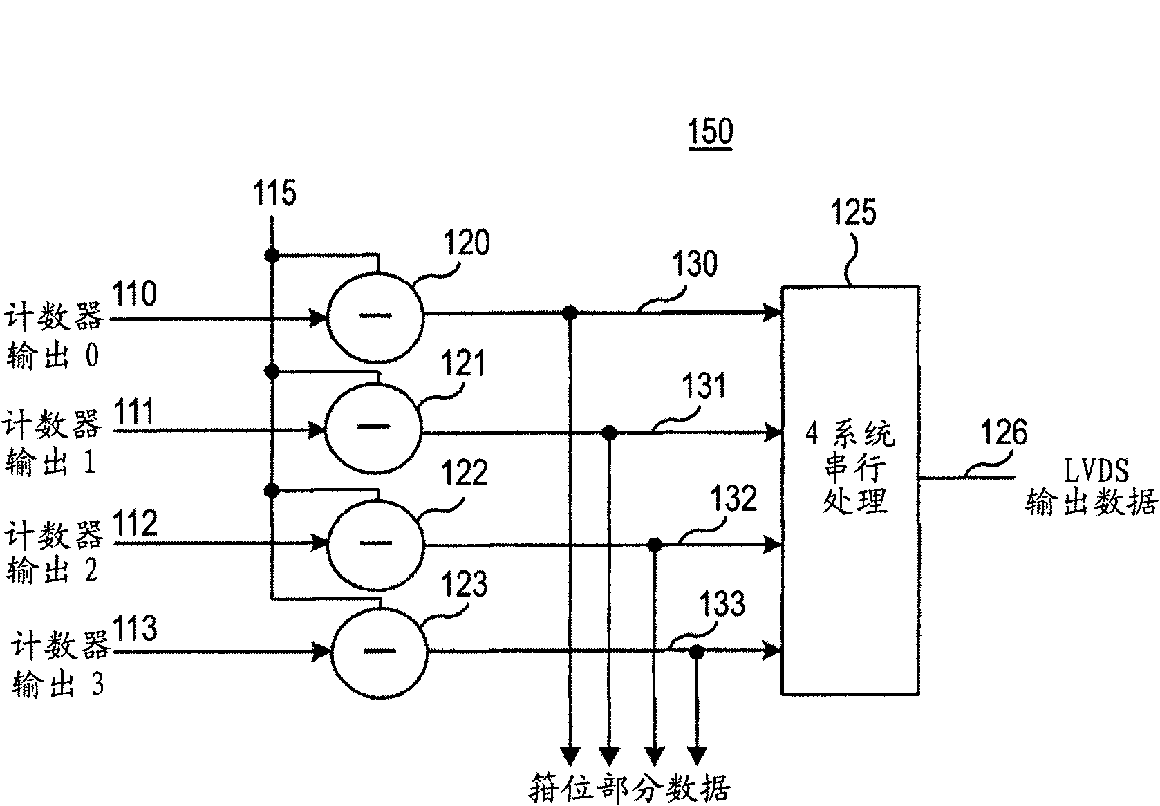
[0025] 2. The specific circuit of the main circuit in the black level correction circuit

[0026] 3. Description of the operation of the black level correction circuit

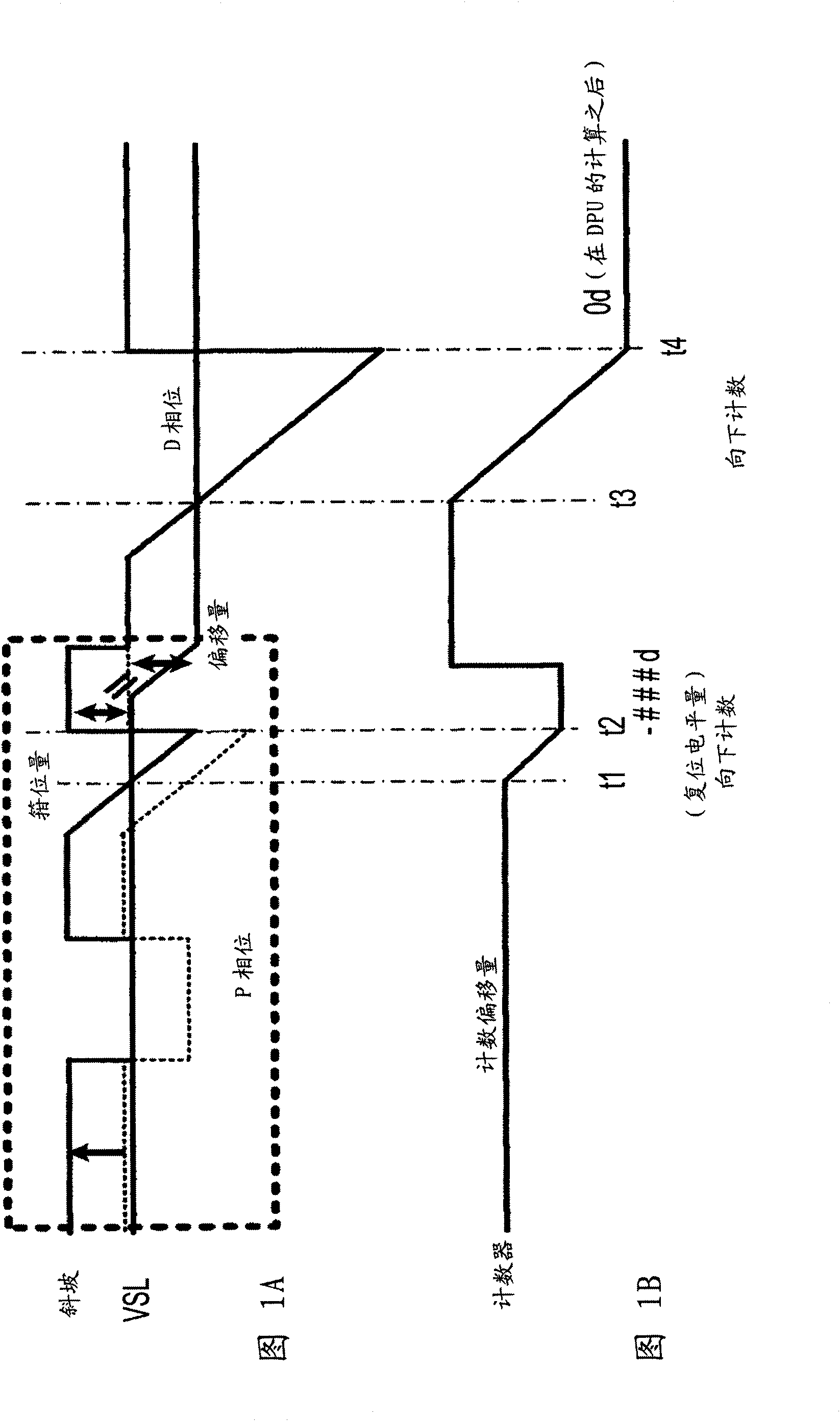
[0027] Figure 1A and Figure 1B Waveform diagrams representing the operation of the solid-state imaging device are shown. The output waveform after CDS (Correlated Double Sampling) is shown. A CDS circuit not shown processes the difference between the precharge phase (P phase) and the data phase (D phase) which is an output signal of the pixel using a sample-and-hold clamp pulse to form a CCD (Charge Coupled Device ) waveform output signal.

[0028] Figure 1A Examples of ramp (Ramp) waveforms in the P phase and D phase are shown. The area surrounded by the dotted line shows the P phase, and the ...


PUM


Abstract

A black level correction circuit includes: a counter counting a black signal level of an image; a black level determination section determining a feedback gain by comparing data outputted from the counter with a previously set threshold; an average value calculation section calculating an average value from data supplied from the counter; a feedback calculation processing section selecting the feedback gain by a control signal supplied from the black level determination section and calculating the selected feedback gain and the averaged data; and a digital-analog converter correcting data to which feedback calculation processing has been performed and converting the corrected data into analog data to output an analog black signal.

Description

technical field [0001] The present invention relates to a black level correction circuit for solid-state imaging devices and the like, and more particularly to a clamp circuit for correcting blocked up shadows. Background technique [0002] In a clamp circuit, the black level is generally maintained constant by detecting a difference from a target value and feeding the difference back to a DAC (Digital-to-Analog Converter) section. However, at the time of detection, there are cases where there are many dots having levels significantly higher than the target black level in levels where white point removal is not performed; and where patterns such as frames ( pattern) is included in the calculation range. In these cases, the black level in the clamping range becomes higher than that in the effective pixel area, which unnecessarily increases the control value for the DAC section. [0003] As a result, excessive drawing is performed, and when the black level is displayed in 8 ...

Claims


Application Information

Patent Timeline
Patent Type & Authority Applications(China)
IPC IPC(8): H04N5/217H04N5/335H04N5/369H04N5/374H04N5/378
CPCH04N5/361H04N5/185H04N25/63
Inventor 堀川裕之宇井博贵
Owner SONY GRP CORP
Learn More