
Nonvolatile semiconductor photorefractive memory structure

A non-volatile, semiconductor technology, applied in the field of medium refractive index, can solve the problems of small coupling part, low efficiency, weak refractive index of optical waveguide, etc., and achieve the effect of energy saving, high efficiency and broad application prospects

Inactive Publication Date: 2011-07-27
JILIN UNIV
View PDF0 Cites 1 Cited by
  • Summary
  • Abstract
  • Description
  • Claims
  • Application Information

AI Technical Summary

Problems solved by technology

[0005] The prior art close to the structure of the present invention is an optical read-only memory paper published by Cornell University in 2006: C.A.Barrios and M.Lipson, "Silicon Photonic Read-Only Memory," J.of Lightwave Thechnol. 242006 pp2898, in the structure designed in the paper, the floating gate and the optical waveguide are separated, the coupling part of the carrier and light in the floating gate is small, and the efficiency is low; in the structure designed in the paper, the optical waveguide is connected to the electrode at the same time, It is used as an electrode, so the area of ​​the floating gate is limited by the area of ​​the waveguide, and the modulation of the refractive index of the optical waveguide is very weak

Method used


Image

  • Nonvolatile semiconductor photorefractive memory structure
  • Nonvolatile semiconductor photorefractive memory structure
  • Nonvolatile semiconductor photorefractive memory structure

Examples


Embodiment 1

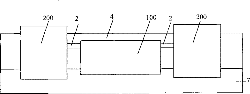
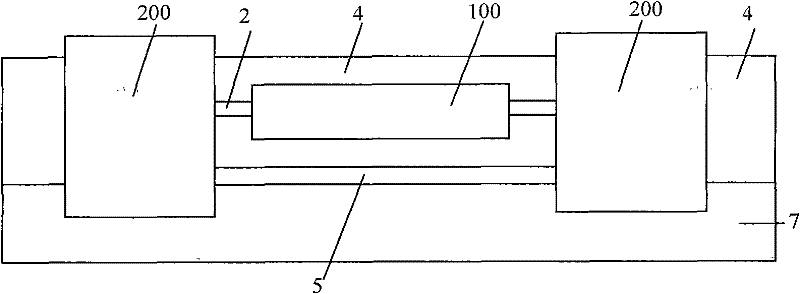
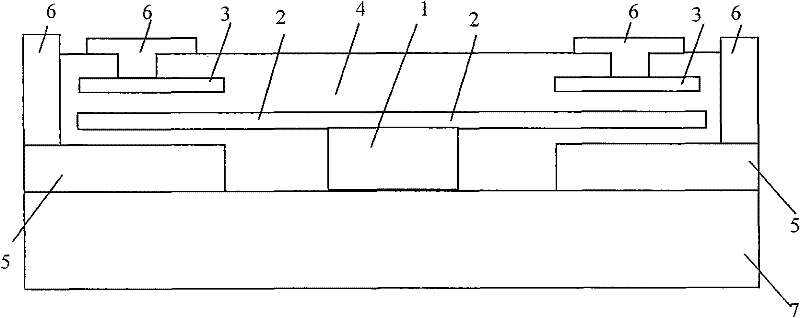
[0028] Example 1 Overall structure of the present invention

[0029] figure 1 , 2 , 3 gives the overall structure of the present invention from different angles. In the figure, 100 is the optical waveguide part, 200 is the floating gate part, 1 is the semiconductor optical waveguide, 2 is the floating gate, 3 is the control gate, 4 is the upper insulator medium, 5 is the conductive medium, 6 is the electrode, 7 is the lower insulator medium.

[0030] The nonvolatile semiconductor photorefractive memory structure of the present invention is composed of an optical waveguide part 100 and a floating gate part 200. in figure 1 , 2 In the structure shown in 3, there are two floating gate portions 200. Among them, the optical waveguide section 100 is composed of a semiconductor optical waveguide 1, an upper insulator medium 4 above the semiconductor optical waveguide 1, and a lower insulator medium 7 below the semiconductor optical waveguide 1; the floating gate section 200 is made up o...

Embodiment 2

[0033] Embodiment 2 Different structure of optical waveguide part 100

[0034] Figure 4 , 5 , 6, and 7 respectively show the optical waveguide part 100 of different structures.

[0035] Figure 4 As shown, the semiconductor optical waveguide 1 is a strip waveguide, the floating gate 2 is in direct contact with the semiconductor optical waveguide 1, and the floating gates 2 in the two floating gate portions are connected together. The upper insulator medium 4 and the lower insulator medium 7 electrically isolate the semiconductor optical waveguide 1 and the floating gate 2 from other components.

[0036] Figure 5 As shown, the semiconductor optical waveguide 1 is a ridge waveguide, the floating gate 2 is in direct contact with the semiconductor optical waveguide 1 on the ridge of the semiconductor optical waveguide 1, and the rest are the same. Figure 4 .

[0037] Image 6 As shown, the semiconductor optical waveguide 1 is an inverted ridge waveguide, the floating gate 2 is in direc...

Embodiment 3

[0040] Embodiment 3 Different structures of floating gate portion 200

[0041] Figure 8 with Picture 9 The structure of one floating gate portion 200 is drawn each. The position of each component is that one electrode 6 contacts the control gate 3, the floating gate 2 is underneath, and the conductive medium 5 is underneath. The conductive medium 5 is in contact with the other electrode 6; the floating gate 2, the control gate 3 and the conductive medium 5 are connected from above. The insulator medium 4 is electrically isolated.

[0042] Figure 8 versus Picture 9 The only difference is that the conductive medium 5 is only in its own floating gate part 200 (such as Figure 8 Shown) and the conductive medium 5 stretched out of its own floating gate portion 200 (such as Picture 9 The middle conductive medium 5 is shown at the left end), which can be integrated with another conductive medium 5 and electrically isolated from the semiconductor optical waveguide 1.


PUM


Abstract

The invention belongs to the technical field of semiconductor electric devices. The structure comprises an optical waveguide part (100) and a floating gate part (200), wherein the optical waveguide part comprises a semiconductor optical waveguide (1), an upper insulator medium (4) and a lower insulator medium (7); the floating gate part (200) comprises floating gates (2), control gates (3), conducting mediums (5) and binate electrodes (6); the floating gates (2) are arranged between the control gates (3) and the conducting mediums (5), and are isolated by the upper insulator medium (4); and the floating gates (2) are contacted with the semiconductor optical waveguide (1). In the invention, the semiconductor optical waveguide has the function of charge storage memory of the floating gates;meanwhile, charge has modulating action on the index of refraction of the optical waveguide. When the invention is applied to an optical switch, pulse energy is additionally added for control only when the state of the optical switch is changed, and a lot of energy is saved. When the invention is applied to a photonic micro-cavity, resonance condition in the micro-cavity has memorability.

Description

Technical field: [0001] The invention belongs to the technical field of semiconductor optoelectronic devices, and particularly relates to the refractive index of a medium in an integrated optical device. Background technique: [0002] With the rapid popularization of optical communication network technology, the energy consumption for optical switching and optical transmission is also increasing. Therefore, the demand for low-energy devices in optical networks is becoming more and more urgent. The optical switching system composed of optical switches is a key part of the optical network. It provides an optical link that transmits an optical signal from a certain entrance to a certain exit. After an optical link is established and before it is changed, the state of the optical link does not change, but the voltage (or current) that controls each optical switch must be kept working to keep this optical link open. If we can make each optical switch have the storage function of ele...

Claims


Application Information

Patent Timeline
Patent Type & Authority Patents(China)
IPC IPC(8): H01L27/115H01L29/792H01L29/51H10B69/00
Inventor 宋俊峰卢国强
Owner JILIN UNIV
Learn More