PCB encapsulation of surface patch capacitor, method thereof, PCB and equipment

A printed circuit board and surface mount technology, which is applied in the direction of assembling printed circuits with electrical components, printed circuits connected with non-printed electrical components, and the formation of electrical connections of printed components, can solve the problem of increased capacitance distribution, inductance, and capacitance filtering Effect reduction and other issues, to achieve the effect of reducing distributed inductance, improving effect, and saving design workload

Inactive Publication Date: 2010-11-10
BEIJING XINWANG RUIJIE NETWORK TECH CO LTD
View PDF3 Cites 9 Cited by
  • Summary
  • Abstract
  • Description
  • Claims
  • Application Information

AI Technical Summary

Problems solved by technology

[0005] The purpose of the present invention is to provide a PCB package of surface mount capacitors and its method, printed circuit board and equipment, which can solve the problems in the prior art that the distributed inductance from the capacitor to the power supply or ground plane increases, which leads to the reduction of the filtering effect of the capacitor, etc. question

Method used


Image

  • PCB encapsulation of surface patch capacitor, method thereof, PCB and equipment
  • PCB encapsulation of surface patch capacitor, method thereof, PCB and equipment
  • PCB encapsulation of surface patch capacitor, method thereof, PCB and equipment

Examples


Embodiment 1

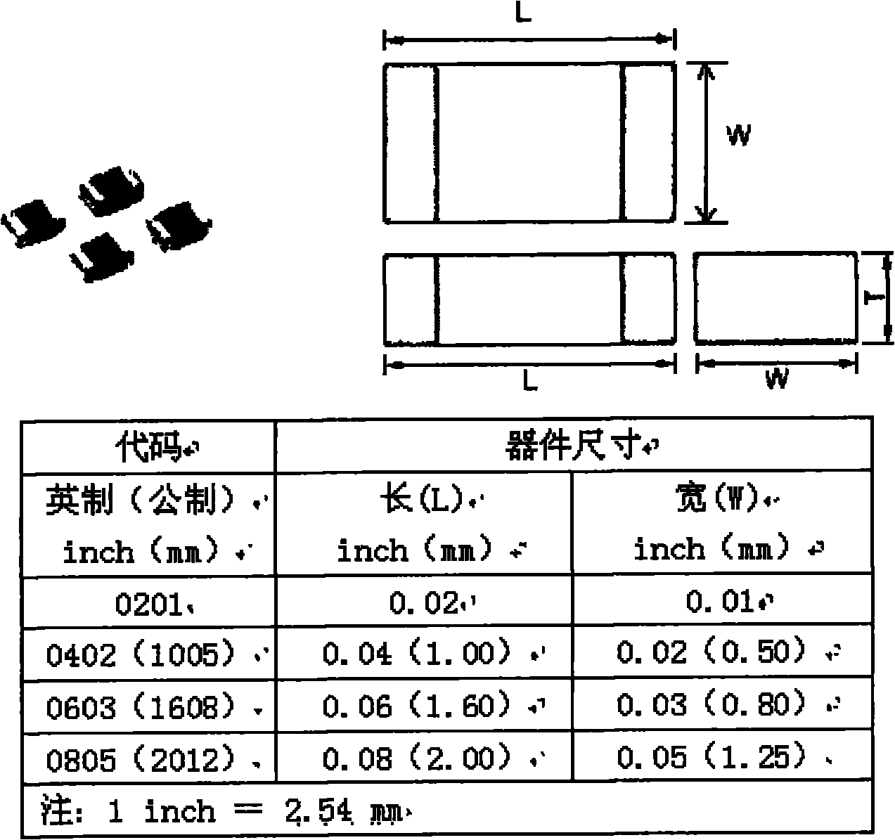
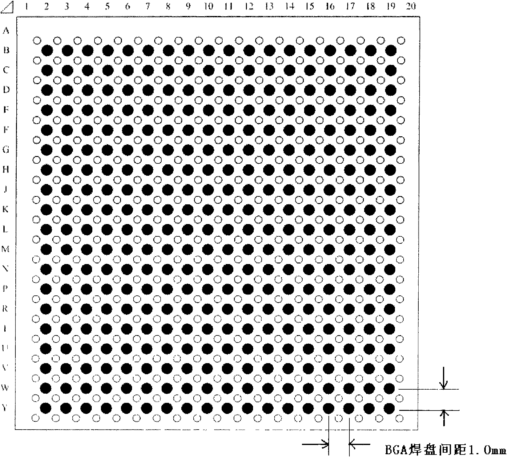
[0051] Preferred embodiment one: take 0402 SMT electric capacity, the pad pitch of BGA chip is 1.0mm as example, the PCB encapsulation method of SMT electric capacity of the present invention mainly comprises the following steps:

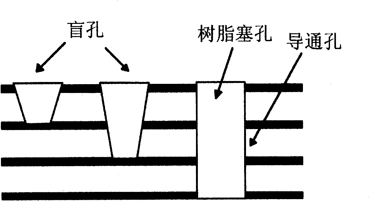
[0052] Step 1, create a new 0402 PCB package design: adjust the value of the standard 0402 pad to get a package with new pad width, pad length and two pad spacing values, so that on the pad Add vias. If the via hole adopts laser blind hole or mechanical via hole with an outer diameter of 18mil, it is not necessary to adjust the standard PCB package size of 0402; if the PCB board is thick, a mechanical via with an outer diameter of ≥20mil is required. For through holes, the width, length and spacing of the two pads need to be adjusted accordingly.

[0053] Step 2, add a via hole on each of the two pads of the capacitor, and adjust the position of the via hole according to the PCB package size of 0402 and the BGA pad spacing of 1.0mm. The via hole c...


PUM


Abstract

The invention provides PCB encapsulation of a surface patch capacitor, a method thereof, a PCB and equipment. The PCB encapsulation of the surface patch capacitor is arranged on the PCB of a ball grid array chip. The PCB encapsulation method comprises the following steps of: adjusting the sizes of bonding pads of a surface patch capacitor in the standard encapsulation size according to the set sizes of via holes and a making process; arranging via holes in the two bonding pads of the surface patch capacitor, wherein the number of the via holes is confirmed according to the sizes of the bonding pads of the surface patch capacitor, and the positions of the via holes are confirmed according to the sizes of the bonding pads of the surface patch capacitor and the bonding pad distance of the ball grid array chip.

Description

technical field [0001] The invention relates to the field of printed circuit boards, in particular to a PCB package of surface mount capacitors, a method thereof, a printed circuit board and equipment. Background technique [0002] With the continuous improvement of the integration of electronic products, electronic components have been continuously miniaturized. Semiconductor technology and SMT (Surface Mount Tech, surface mount) technology have been developed so far, and ball grid array packaging technology (Ball Grid Array Package, BGA packaging) is adopted chips have been widely used. While this technology keeps electronic products miniaturized, it also brings various new technical challenges to the realization of design and manufacture. For example, the power filter processing of BGA chip, in order to achieve the design index of power integrity and ensure the stable and reliable operation of the chip, each power pin is required to place a filter capacitor. Generally, S...

Claims


Application Information

Patent Timeline
Patent Type & Authority Applications(China)
IPC IPC(8): H05K3/30H05K3/42H05K1/18H01L23/48
CPCY02P70/50
Inventor 张华民
Owner BEIJING XINWANG RUIJIE NETWORK TECH CO LTD
Why Eureka
Try Eureka