Broadband all-dielectric multilayer-film reflective diffraction grating and design method thereof

A reflection-diffraction, all-dielectric technology, applied in the field of gratings, can solve problems such as limiting the ability of gratings to resist laser damage and destroying beam wavefronts

Inactive Publication Date: 2010-11-17
SHANGHAI INST OF OPTICS & FINE MECHANICS CHINESE ACAD OF SCI
View PDF3 Cites 37 Cited by
  • Summary
  • Abstract
  • Description
  • Claims
  • Application Information

AI Technical Summary

Problems solved by technology

However, due to the introduction of metal materials, the inherent absorption characteristics of metal materials will limit the laser damage resistance of this type of grating to a

Method used


Image

  • Broadband all-dielectric multilayer-film reflective diffraction grating and design method thereof
  • Broadband all-dielectric multilayer-film reflective diffraction grating and design method thereof
  • Broadband all-dielectric multilayer-film reflective diffraction grating and design method thereof

Examples


example 1

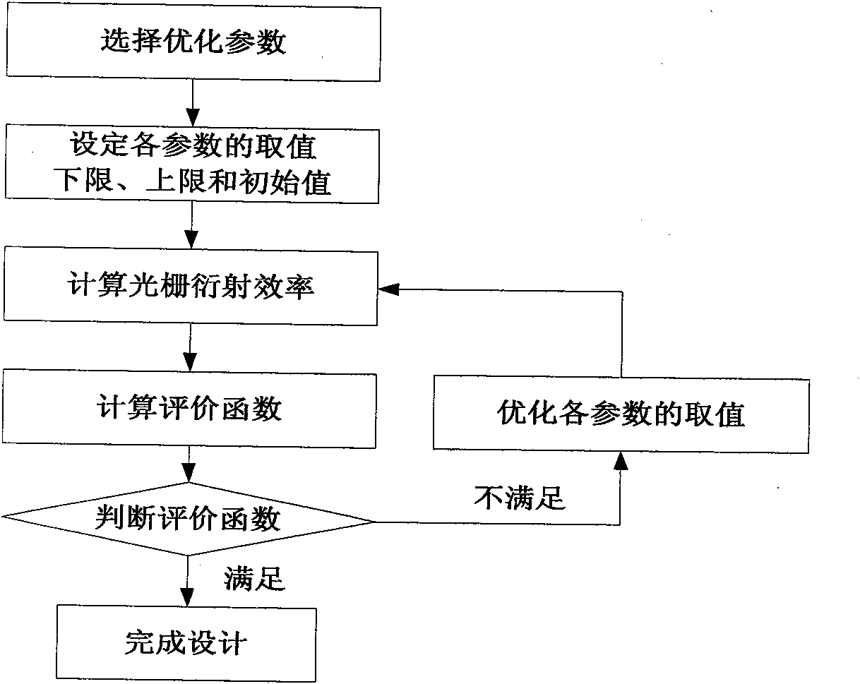
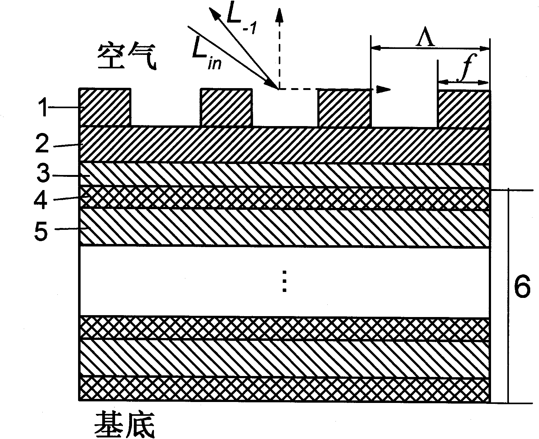
[0086] The grating uses an angle of 57 degrees. The structure of the multilayer dielectric film used for the broadband all-dielectric multilayer film reflection diffraction grating of the present invention is: S(HL) 9 H M R G A. H and L are the high-refractive index material film layer and the low-refractive index material film layer with the thickness of a quarter of the reference wavelength, respectively, and the HL basic film system is repeated 9 times; M is the matching layer, and G and R are the top-layer etched grating structure layer and the top layer etch the remaining film layers. S is the K9 substrate, and A is the incident air layer. The materials and corresponding refractive indices of each layer are as follows:

[0087]

[0088] In this example, the grating period ranges from 480nm to 510nm. The duty cycle ranges from 0.25 to 0.5. The upper and lower limits of grating etching thickness, top layer remaining thickness and matching layer thickness are 300nm,...

example 2

[0095] The grating structure and usage conditions are the same as those in Design Example 1, and the Ta in Design Example 1 2 o 5 Replaced with TiO 2 (refractive index 2.31), other materials remain unchanged. When optimizing the design, the value range of each parameter and the optimization steps are also consistent with the design example one. After multiple optimizations and designs, the minimum rating function value is 1.4358, the corresponding grating period is 510nm, and the duty ratio is 0.25. The etching thickness of the grating, the remaining thickness of the top layer and the thickness of the matching layer are 210nm, 11nm and 18nm, respectively. The reference wavelength is 834nm.

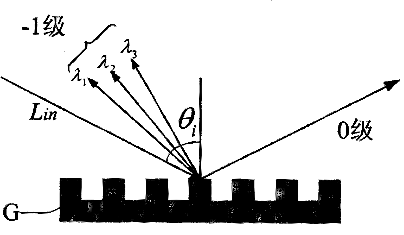
[0096] Figure 4 It is the broadband diffraction spectrum of the broadband all-dielectric multilayer reflection diffraction grating of the present invention. With 800nm ​​as the center wavelength, the diffraction efficiency of the grating exceeds 98% and the bandwidth exceeds 100nm. ...


PUM

PropertyMeasurementUnit
Thicknessaaaaaaaaaa
Thicknessaaaaaaaaaa

Abstract

The invention provides a broadband all-dielectric multilayer-film reflective diffraction grating and a design method thereof. The broadband all-dielectric multilayer-film reflective diffraction grating comprises a base, a high film reflecting layer and a grating layer, wherein the high film reflecting layer and the grating layer are formed by periodic alternation of a high-refractive index material and a low-refractive index material. The invention is characterized in that a matching layer and a residual film layer are arranged between the high film reflecting layer and the grating layer; the refractive index of the material of the matching layer is as the same as the low-refractive index material in the high film reflecting layer; the refractive index of the material of the grating layer and the material for etching the residual film layer is less than that of the high-refractive index material; and the period and the duty cycle and the etching depth of the grating layer, the thickness of the residual film layer, the thickness of the matching layer and the wavelength control value for preparing the high film reflecting layer are correlated and determined by a multi-parameter optimization design. In the invention, the diffraction efficiency of the broadband all-dielectric multilayer-film reflective diffraction grating is more than 97.5% when an incident TE polarized light approaches within the range of more than 100nm spectral bandwidth in a 1-grade reflective diffraction direction.

Description

technical field [0001] The invention relates to a grating, in particular to a wide-band all-dielectric multi-layer reflection diffraction grating and a design method thereof. Background technique [0002] High-power ultrashort pulse lasers based on chirped pulse amplification technology have a wide range of application requirements in the fields of laser processing and research on the interaction between light and matter. As the core component of the chirped pulse amplification technology, the all-dielectric multilayer grating has the advantages of high diffraction efficiency and high resistance to laser damage, which is very beneficial to improving the output power of the pulsed laser system and prolonging the service life of the laser system. As the laser pulse width narrows, the spectral width widens accordingly. For example, if the pulse width reaches the femtosecond level, the corresponding spectral width can exceed 100nm. Then, the grating used for pulse compression an...

Claims


Application Information

Patent Timeline
IPC IPC(8): G02B5/18G02B27/00
Inventor 汪剑鹏晋云霞刘娜李淑红范正修
Owner SHANGHAI INST OF OPTICS & FINE MECHANICS CHINESE ACAD OF SCI
Why Eureka
Try Eureka