Method for wafer test and probe card for the same

A technology of wafer testing and probe card, which is applied to the components of electrical measuring instruments, semiconductor/solid-state device testing/measurement, electrical measurement, etc., which can solve the problem of thermal deformation of probe card, deterioration of probe card alignment accuracy and Flatness, unstable contact and other problems, to achieve the effect of reducing the number of tests and effectively improving the test

Active Publication Date: 2010-11-17
AMST CO LTD
View PDF0 Cites 16 Cited by
  • Summary
  • Abstract
  • Description
  • Claims
  • Application Information

AI Technical Summary

Problems solved by technology

The end result is a possible asymmetrical thermal deformation of the corresponding probe card during each touchdown
Thermal deformation can deteriorate the alignment accuracy and planarity of the probe card, which can lead to unstable contact between the probe card and the wafer, resulting in unreliable test results
In addition, there are a large number of probes that do not participate in the test when testing various areas, resulting in a decrease in the efficiency of test resource usage

Method used


Image

  • Method for wafer test and probe card for the same
  • Method for wafer test and probe card for the same
  • Method for wafer test and probe card for the same

Examples


Embodiment approach

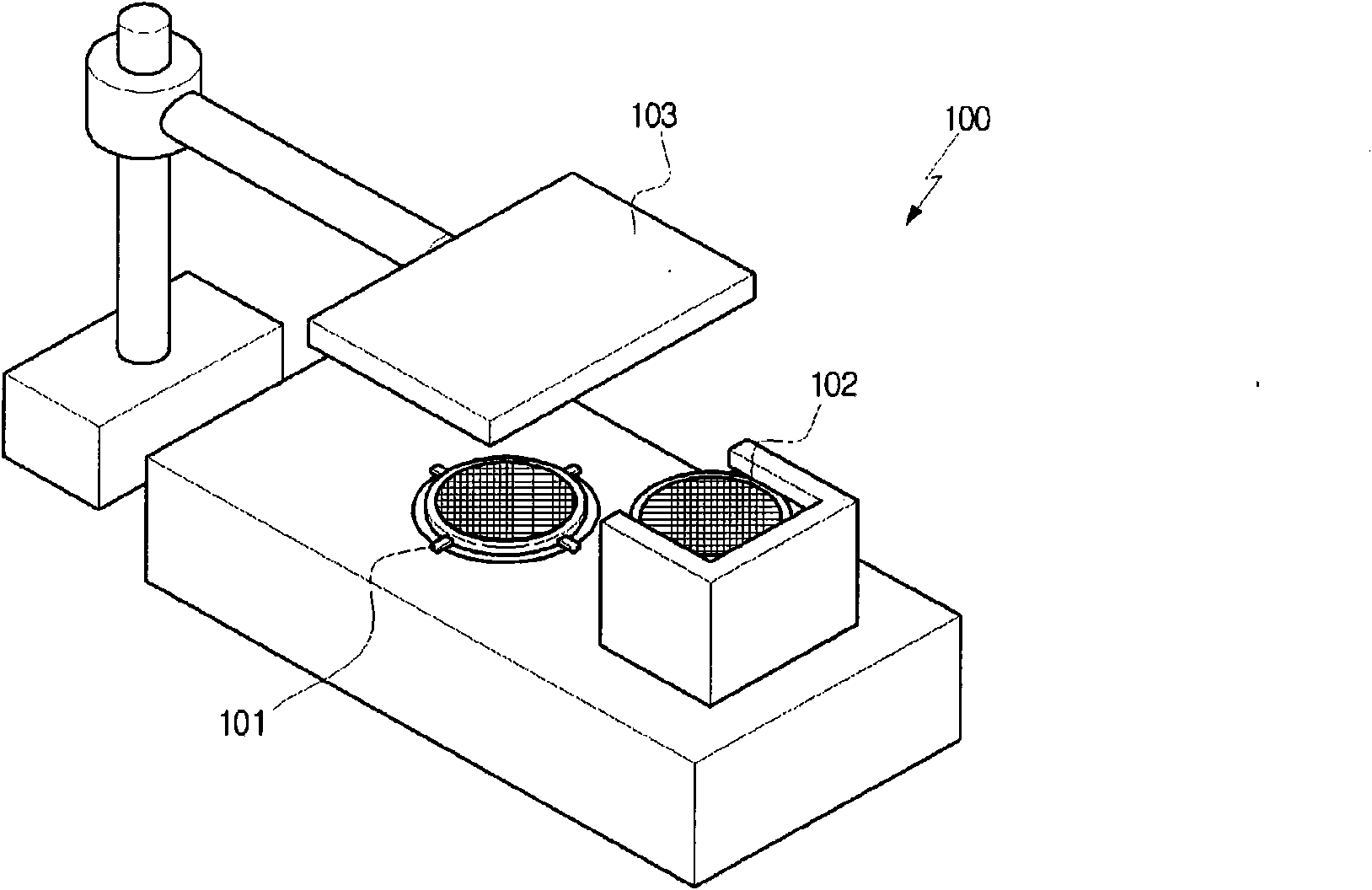
[0044] Hereinafter, a method of testing a wafer according to an embodiment and a probe card used for the method will be described in detail with reference to the accompanying drawings.

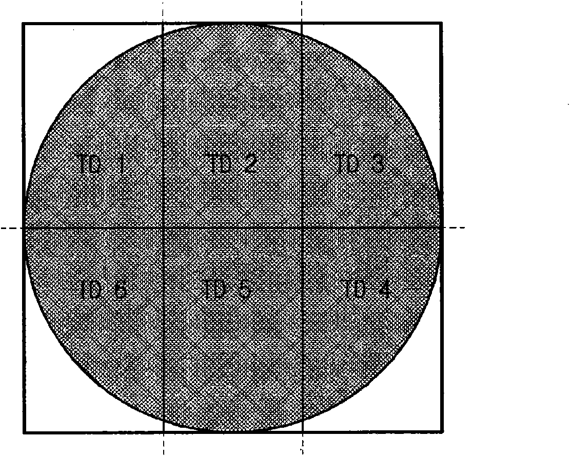
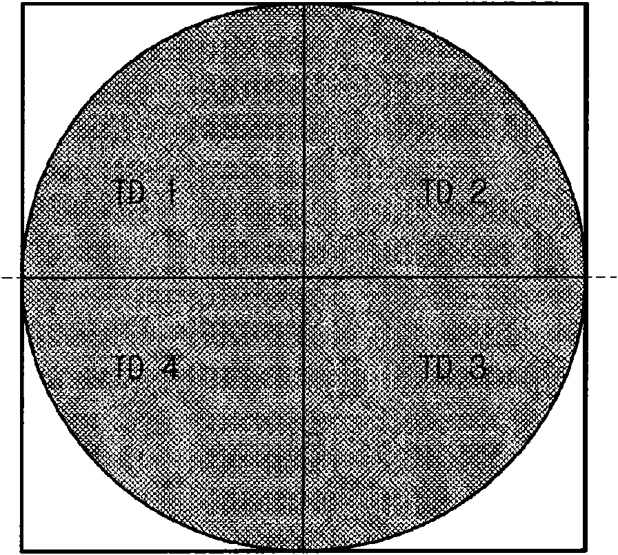
[0045] In order to implement the wafer testing method disclosed herein, firstly, the concept of repeating unit is applied to the semiconductor chips of the wafer to be tested. A plurality of semiconductor chips are arranged on the wafer. A semiconductor chip is defined as a group of repeating units and the repeating unit is defined as a plurality of groups of N adjacent semiconductor chips. N is a natural number not less than 2, for example, N is a natural number between 2 and 50. For example, in Figure 4 Among them, the semiconductor chip C of the wafer 600 can be defined as a set of repeating units 610 composed of four semiconductor chips C. At this point, adjacent repeating units can share some chips. For example, when a first repeating unit and a second repeating unit are defined on a...


PUM


Abstract

A method of testing a wafer capable of minimizing the asymmetrical thermal deformation of a probe card when a wafer is tested using a probe card and of minimizing the number of times of tests to effectively test a large area wafer and a probe card for the same is presented. For the wafer test method for testing semiconductor chips on a wafer using a probe card, the method includes creating virtual repeating units corresponding to N semiconductor chips, wherein the N is natural number larger than or equal to 2, arranging the plurality of repeating units on the wafer and moving the probe card or the wafer N times and testing the semiconductor chips on a wafer, wherein the semiconductor chips in the repeating units are sequentially tested one by one per each touchdown. Also, the probe cards to realize above mentioned method have been described.

Description

technical field [0001] The following description relates to a method of testing a wafer and a probe card used for the method, and more particularly, to a method capable of minimizing asymmetric thermal deformation of the probe card during wafer testing using the probe card. A method of optimizing and minimizing the number of touchdowns of a probe card to efficiently test a large-area wafer, and a probe card used for the method. Background technique [0002] Generally, a semiconductor manufacturing process is divided into a front-end process and a back-end process. The front-end process, which is a manufacturing process, is a process for forming integrated circuit patterns on a wafer. The back-end process, which is an assembly process, is a process for forming integrated circuit packages by dividing the wafer into chips, connecting conductive leads or balls to each chip to provide electrical paths to external devices, and then using Epoxy molded chips. [0003] Before perf...

Claims


Application Information

Patent Timeline
Patent Type & Authority Applications(China)
IPC IPC(8): H01L21/66
CPCG01R31/2887G01R1/0491
Inventor 郑仁范宋柄昌金东日
Owner AMST CO LTD
Why Eureka
Try Eureka