

Self-adhesive mica tape winding wire
A mica tape, self-adhesive technology, applied in the direction of flat/ribbon cables, insulators, manufacturing motor generators, etc., can solve the problems of complex structure, damage to environmental protection, unreasonable consumption of raw materials, etc., to avoid environmental damage Influence, reduce the effect of process steps
- Summary
- Abstract
- Description
- Claims
- Application Information
AI Technical Summary
Problems solved by technology
Method used
Image

Examples
Embodiment 1
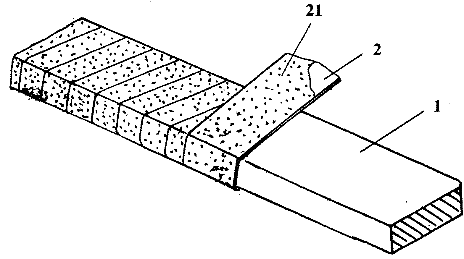
[0028] please see figure 1 ,exist figure 1 The conductor 1 given in is a flat copper conductor with a thickness of 5.5mm and a width of 15.5mm. An insulator is combined outside the conductor 1. In this embodiment, a self-adhesive layer is coated on one side. The first mica tape 2 of 21 is used as an insulator, and the first mica tape 2 is wrapped on the conductor 1 in an overlapping manner. When wrapping, the side with the self-adhesive layer 21 faces away from the conductor 1, that is to say, With the self-adhesive layer 21 facing outwards. The thickness of the first mica tape 2 is 0.09mm, and the wrapping ratio is 66%. The so-called wrapping ratio can also be referred to as the overlapping ratio, which refers to the ratio of the width of the overlapping portion to the width of the first mica tape 2. The encapsulation rate is also the preferred value obtained by the applicant through repeated trials, because the overlapping part will cause unnecessary (unreasonable) waste o...
Embodiment 2
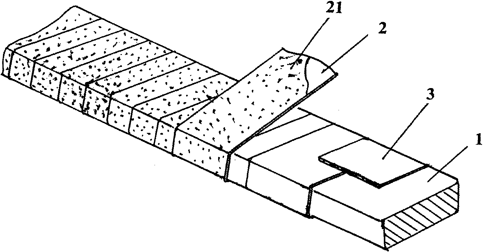
[0032] please see figure 2 , by wrapping the film 3 outside the flat copper conductor 1, the film 3 adopts a polyimide film with a thickness of 0.04mm, and then wraps the surface of one side of the polyimide film in combination with a self-adhesive layer 21 The first mica tape 2 , that is to say, in this embodiment, the film 3 and the first mica tape 2 jointly constitute the insulator. Wherein: the thickness of the conductor 1 is 1mm, and the width is 2.5mm, the thickness of the first mica tape 2 is 0.09mm, the wrapping rate of the first mica tape 2 is 50%, all the other are the same as the description to embodiment 1.
Embodiment 3
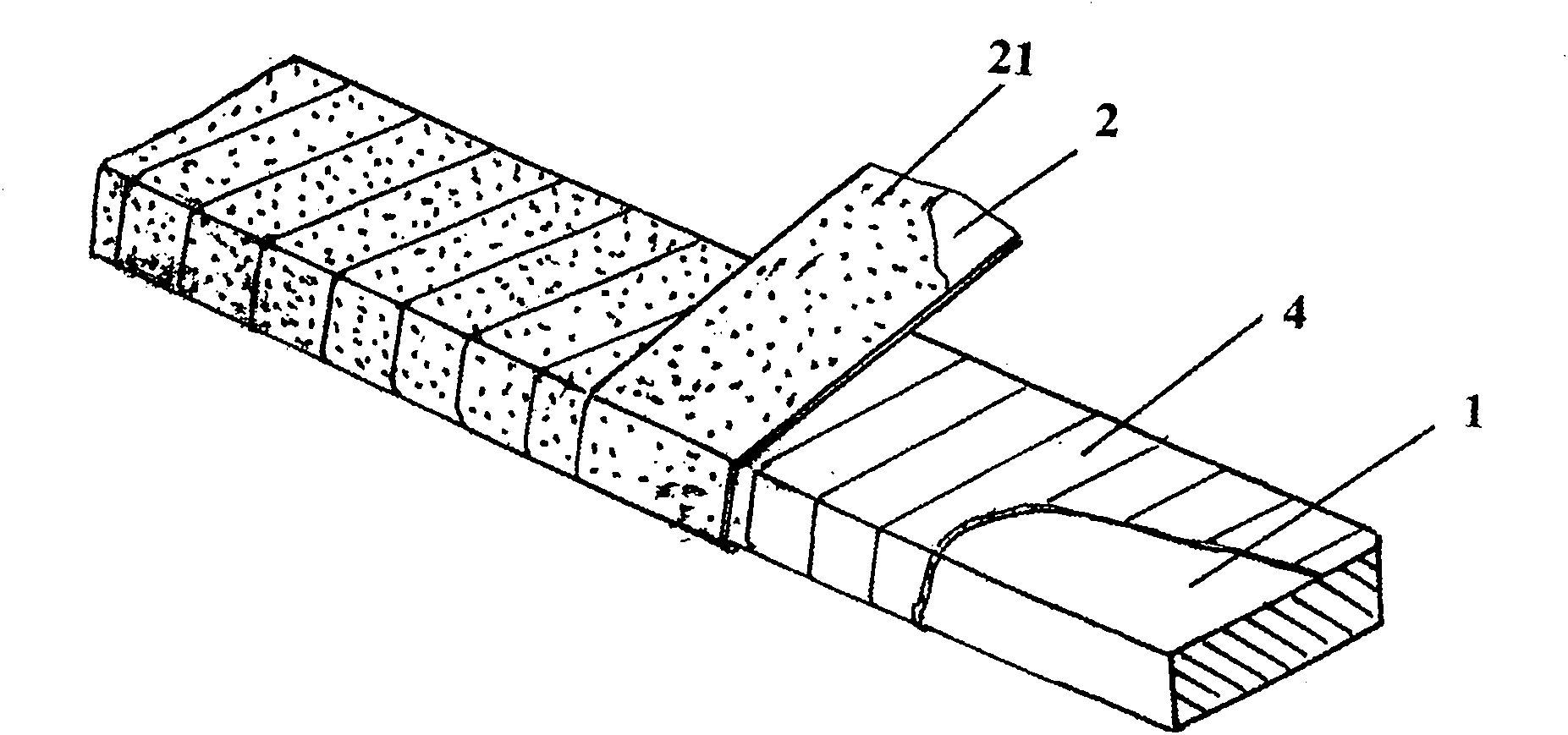
[0034] please see image 3 , sintering and bonding the encapsulation layer 4 by sintering the flat copper conductor 1 with a thickness of 3 mm and a width of 10 mm, and then wrapping the encapsulation layer 4 on one side surface with a self-adhesive layer 21 First mica tape 2. It can be seen that in this embodiment, the encapsulation layer 4 and the first mica tape 2 jointly constitute an insulator combined outside the conductor 1 . Wherein: the thickness of the first mica tape 2 is 0.08mm, the wrapping rate of the first mica tape 2 is 50%, and the encapsulation layer 4 is polyamide coated with a composite film coated with fluorine 46 (F46) on one or both sides. Imine film, all the other are the same as the description to embodiment 1.
PUM
| Property | Measurement | Unit |
|---|---|---|
| Thickness | aaaaa | aaaaa |
| Width | aaaaa | aaaaa |
| Thickness | aaaaa | aaaaa |
Abstract
Description
Claims
Application Information