Non-contact synchronous measuring instrument for subgrade and rail vibration

A synchronous measurement, non-contact technology, used in instruments, measuring devices, measuring ultrasonic/sonic/infrasonic waves, etc., can solve the problems of large error, low precision, and cumbersome testing methods, achieve intelligentization, avoid precision reduction, and eliminate The effect of human factors

Inactive Publication Date: 2010-12-15
TIANJIN UNIV
2 Cites 2 Cited by

AI-Extracted Technical Summary

Problems solved by technology

This measurement method has low precision, ...

Abstract

The invention relates to a non-contact synchronous measuring instrument for subgrade and rail vibration. A CCD (Charge Coupled Device) drive circuit is respectively connected with a CCD video signal binaryzation processing unit, an A/D and SRAM (Static Random Access Memory) working time sequence controller and an address counter time sequence generator and used for providing a necessary working pulse for a CCD and generating an interface signal between the CCD drive circuit and a data acquisition card; and the output of the CCD video signal binaryzation processing unit and the outputs of the A/D and SRAM working time sequence controller and the address counter time sequence generator are connected with a data acquisition interface circuit based on a parallel interface. By computer control automatic measurement, the invention greatly prevents the influence of human factors, realizes the intellectualization of detection, solves the synchronous problem of two different vibration frequencies and vibration amplitudes by non-contact synchronous measurement and can carry out software calibration at random, thereby preventing precision reduction caused by long-term use. A photoelectric probe is just dedusted regularly without replacing a detecting probe regularly.

Application Domain

Technology Topic

Image

  • Non-contact synchronous measuring instrument for subgrade and rail vibration
  • Non-contact synchronous measuring instrument for subgrade and rail vibration
  • Non-contact synchronous measuring instrument for subgrade and rail vibration

Examples

  • Experimental program(1)

Example Embodiment

[0035] The non-contact synchronous measurement instrument for roadbed and rail vibration of the present invention will be described in detail below in conjunction with the embodiments and the drawings.
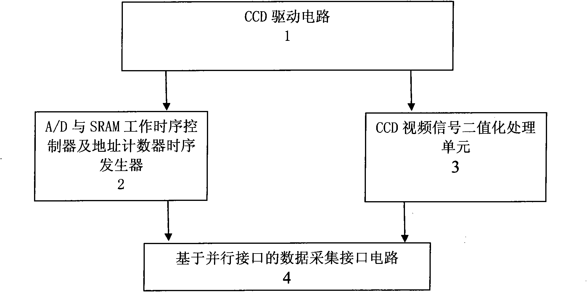
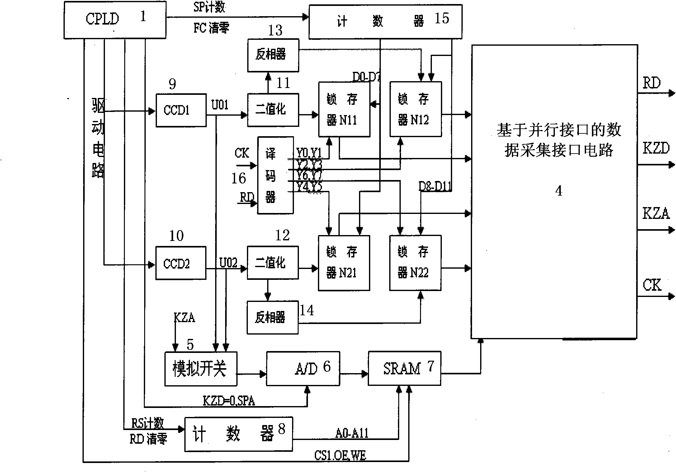
[0036] Such as figure 1 As shown, the non-contact synchronous measuring instrument for roadbed and rail vibration of the present invention includes a CCD drive circuit 1, A/D and SRAM working timing controller, address counter timing generator 2, CCD video signal binarization processing unit 3 And a data acquisition interface circuit 4 based on a parallel interface, wherein the CCD drive circuit 1 is connected to the CCD video signal binarization processing unit 3 and the A/D and SRAM working timing controller and the address counter timing generator 2, respectively, The CCD device provides the necessary working pulses and generates the interface signal with the data acquisition card; the output of the CCD video signal binarization processing unit 3, the A/D and SRAM working timing controller and the address counter timing generator The output of 2 is connected to the data acquisition interface circuit 4 based on the parallel interface.
[0037] The CCD driving circuit 1 uses a field programmable logic device CPLD. The internal logic circuit of CPLD can be used as image 3 The logic circuit shown. image 3 It consists of resistors R1 and R2, inverters T1 and T2, and quartz crystal oscillator Z 1 The constituted oscillator generates a master clock pulse with a frequency of f and the frequency divided by the frequency divider is respectively f 1 , F 2 , F 3 The pulses are passed through the inverter T 7 , T 8 , T 9 And T 10 Logic circuit generated versus Pulse signal, Via inverter T 10 After being reversed, it is sent to the input terminal of the N-bit binary counter. Q in the counter 0 Drive pulse Phaser T 11 Obtained after inversion The transfer pulse SH is obtained by using the J and P output terminals Q of the N-bit binary counter J With Q P After the phase AND causes the counter to count up to 2236 reset pulses RS, the AND gate outputs a high level, and then phases with RS to generate the reset pulse R of the N-bit binary counter to reset the N-bit binary counter, and then the inverter T 4 Transfer pulse signal.
[0038] Transfer pulse Drive pulse versus Reset pulse These four driving pulses are generated and then reversed and added to the corresponding pins of the first linear array CCD19 and the second linear array CCD210 of the model TCD1206SUP in the CCD video signal binarization processing unit 3.
[0039] The A/D and SRAM working timing controller and address counter timing generator 2 include: an analog switch 5 connected to the CCD video signal binarization processing unit 3, and an A/D converter connected to the CCD driving circuit 1 respectively 6. SRAM 7 and counter 8, said analog switch 5, A/D converter 6 and SRAM 7 are also connected in turn, said counter 8 output is connected to SRAM 7, said SRAM 7 is connected to data acquisition interface circuit 4 based on parallel interface .
[0040] The A/D conversion 6 is completed by the 8-bit high-speed video A/D conversion chip CA3318CE. This A/D conversion device is fast, and the conversion time is not more than 67ns. The highest conversion rate of the A/D conversion chip CA3318CE is 15MHz.
[0041] The CCD video signal binarization processing unit 3 includes two identical first linear array CCD1 9 and second linear array CCD2 10. The first linear array CCD1 (9) and the second linear array CCD2 (10 ) The output signal is divided into two channels for processing, one enters the A/D and SRAM working timing controller and the address counter timing generator 2, and the other enters the binary processing circuit 11/12, the binary processing circuit 11/12 are respectively connected to the inverter 13/14 and the first latch N11/N21, the inverter 13/14 is connected to the second latch N12/N22, and a counter 15 and a decoder 16 are also provided , The counter 15 and the decoder 16 are respectively connected to the first latch N11/N21 and the second latch N12/N22, the first latch N11/N21 and the second latch N12 /N22 are connected to the data acquisition interface circuit 4 based on the parallel interface.
[0042] The binary data acquisition method and the computer interface circuit adopted are the edge data transfer method binary data acquisition interface circuit. Figure 4 Shown is the principle block diagram of the computer interface circuit of the edge data transfer method binarization data acquisition. The binary counter 15 controlled by the 10-line sync pulse Fc of the first linear array CCD19 and the second linear array CCD2 counts the number of standard pulses per line (which can be the reset pulse RS of the CCD or the pixel sampling pulse SP). When the standard pulse is the first When the reset pulse RS or the pixel sampling pulse SP of the linear array CCD19 and the second linear array CCD2 10, the count value of the counter 15 at a certain moment is the linear array first linear array CCD19 and the second linear array CCD2 10 output the image sensitive unit at this moment If the value stored in the counter 15 is latched by the latches N11, N12, N21, and N22 at this moment, then the latches N11, N12, N21, and N22 can combine the first line array CCD19 with the second line The position of a certain characteristic pixel of the array CCD2 10 is output and stored.
[0043] The working pulse waveform of this way is like Figure 5 Shown. In this way, the counter periodically outputs the position number of the pixel. In addition, the first linear array CCD1 9 and the second linear array CCD2 10 output the video signal carrying the vibration image of the measured object through the binarization processing circuit to generate the square wave pulse of the measured signal. The front and back edges of the square wave pulse correspond to At two positions on the first linear array CCD19 and the second linear array CCD2 10. The square wave pulses are sent to two edge signal generating circuits respectively. The circuit generates two rising edges, which correspond to the front and back edges of the square wave pulse respectively, that is, on the first linear array CCD19 and the second linear array CCD2 10. Two positions. Use these two edge pulse signals to make the two memories respectively latch the value N counted by the binary counter at the time of the rising edge 11 And N 12 , Then N 11 Is the position value corresponding to the leading moment of the binarized square wave, N 12 Is the position value corresponding to the trailing edge. At the end of the line cycle, the computer software will separate N 11 And N 12 The value is stored in the computer memory through the parallel printer port. The width information of the binarized square wave pulse and the position information of the measured image on the image plane of the first linear array CCD19 and the second linear array CCD2 10 can be obtained.
[0044] The non-contact synchronous measurement instrument for roadbed and rail vibration of the present invention uses two first linear array CCDs of TCD1206SUP 1 9 and second linear CCD 2 10, and two sets of optical imaging systems respectively carry out synchronous data collection on the vibration signals of the roadbed and the rail. The first linear CCD 1 9 and second linear CCD 2 10 Output the video signal U separately under the action of the drive circuit 01 With U 02. They are divided into two channels for processing, and one is sent to the binarization processing circuit for binarization data acquisition and processing. The other channel is pre-amplified and processed by analog switch (for the first linear CCD 1 9 and second linear CCD 2 10 output video signal U 01 With U 02 Make selection) Send it to the A/D conversion circuit and convert it into a digital signal. The clock pulse circuit generates the start signal SPA of the A/D converter and the address of the data memory SRAM. A certain or several video images can be stored as needed. In the high-speed static memory (SRAM), the image in the SRAM can be sent to the computer through the enhanced parallel port (EPP) for display and processing as needed, so as to observe the first linear CCD separately 1 9 and second linear CCD 2 10 working status.
[0045] Such as Image 6 As shown, the principle of roadbed vibration measurement is completely the same as that of rail vibration measurement.
[0046] The black background and white stripe pattern 17 erected on the outside of the roadbed and the railroad track is imaged onto the photosensitive image surface of the linear CCD 19 through the optical imaging objective lens 18. The output end of the linear CCD 19 will be as Figure 7 Output signal U shown 0.
[0047] SH is the transfer pulse of the linear CCD. This pulse is often used as a horizontal synchronization signal to complete the synchronization control of the CCD and the counter. Under the action of driving pulse, the linear CCD output as shown in the figure U 0 signal. Will U 0 The signal is processed by the binary circuit to get Figure 7 The binary square wave pulse output shown, the leading edge of the pulse corresponds to the black and white side N 1 , And the trailing edge corresponds to the white and black edge N 2. The center value N of the white bar should be
[0048] N ( t ) = N 1 + N 2 2 - - - ( 1 )
[0049] Suppose the initial position of the track when it is not impacted by the locomotive (at t=0) is N(t)=N 0 When the track is excited to vibrate (t≥0), the white bar image on the track will vibrate up and down on the image sensitive unit array of the linear CCD. When the integration time of the linear CCD is much shorter than the orbital vibration period, the linear CCD continuously outputs the video signal U of the white bar image at different positions on the CCD image 0. The video output signal U 0 The binarized square wave signal of each integration time is obtained by the binarization processing circuit, and the track position N(t) value of the integration time is obtained by the binarization data acquisition circuit. The relationship between the value of N(t) and the time displacement of the track S(t) is
[0050] S ( t ) = ( N ( t ) - N 0 ) l β - - - ( 2 )
[0051] Where: 1 is the center distance between two adjacent pixels of the CCD; β is the lateral magnification of the optical imaging system.
[0052] β can be calibrated at any time by the known white bar width W
[0053] β = l ( N 2 - N 1 ) W - - - ( 3 )
[0054] Substituting (1) and (3) into (2) to obtain the time displacement S(t) and the measured value N 1 With N 2 Relationship
[0055] S ( t ) = [ N 1 - N 1 ( 0 ) ] + [ N 2 - N 2 ( 0 ) ] 2 ( N 2 - N 1 ) W - - - ( 4 )
[0056] Using (4), the displacement S(t) of the rail vibration in the vertical direction can be obtained. Continuously collect for a period of time to obtain a series of S(t) values, and expand these S(t) values ​​according to the time period (CCD light integration time) to obtain the orbital vibration waveform diagram. In the embodiment of the present invention, let N 1 (0)=N 1 (0)=0.

PUM

no PUM

Description & Claims & Application Information

We can also present the details of the Description, Claims and Application information to help users get a comprehensive understanding of the technical details of the patent, such as background art, summary of invention, brief description of drawings, description of embodiments, and other original content. On the other hand, users can also determine the specific scope of protection of the technology through the list of claims; as well as understand the changes in the life cycle of the technology with the presentation of the patent timeline. Login to view more.

Similar technology patents

Automatic plugging test machine for solar junction box connector

PendingCN113740648AEliminate the influence of human factorsThe test data is accurateMachine part testingElectric connection testingPhysicsBackplane
Owner:ZHEJIANG JIAMING TIANHEYUAN PHOTOVOLTAIC TECH

Intelligent digestion detection system

InactiveCN107478499AEliminate the influence of human factorsEnsuring Accuracy and ConsistencyMaterial analysis by observing effect on chemical indicatorPreparing sample for investigationDigestionReagent
Owner:宋林涛

Classification and recommendation of technical efficacy words

  • Eliminate the influence of human factors
  • Realize intelligence

Interface testing method and device

InactiveCN103389937AImprove test efficiencyEliminate the influence of human factorsSoftware testing/debuggingComputer hardwareTest efficiency
Owner:TENCENT TECH (SHENZHEN) CO LTD

Method for adjusting ore slurry liquid level and foam thickness of coal flotation machine

InactiveCN110270438AEliminate the influence of human factorsReduce labor intensityFlotationCoalEngineering
Owner:TIANDI TANGSHAN MINING TECH +1

Molding tool and molding method for zero-degree fiber bundles for R-angle reinforcement of composite material

ActiveCN104260371AGuaranteed Dimensional QualityEliminate the influence of human factorsFiber bundleMaterials science
Owner:SHENYANG AIRCRAFT CORP

Intelligent warehouse system

Owner:哈尔滨灵翰智能技术有限公司
Why Eureka
Try Eureka