

Configurable radio-frequency power amplifier and radio-frequency transmitting front-end module with same
A technology of radio frequency power and front-end modules, applied in power amplifiers, sustainable buildings, climate sustainability, etc., can solve the problems of high cost, low integration, and large area of mobile terminals, and achieve the reduction of circuit board area and reduction Quantity, the effect of reducing manufacturing cost
- Summary
- Abstract
- Description
- Claims
- Application Information
AI Technical Summary
Problems solved by technology
Method used
Image

Examples
Embodiment 1
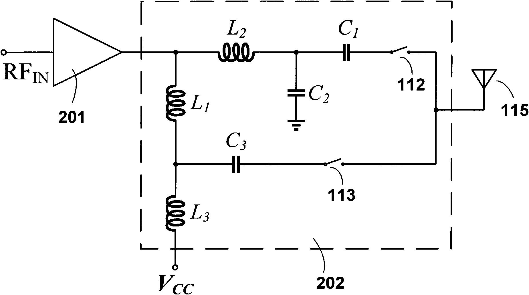
[0036] Such as figure 2 Shown is the implementation of the radio frequency power amplifier with configurable output impedance matching network proposed by the present invention. The radio frequency power amplifier includes a radio frequency power amplifier die 201, a first inductor L1, a second inductor L2, a third inductor L3, a first capacitor C1, a second capacitor C2, a third capacitor C3, a radio frequency switch 112, a radio frequency switch 113 and an antenna 115. The input of the RF power amplifier is connected to the RF input signal (RF IN ), the output end is connected to one end of the first inductance L1 and the second inductance L2; the other end of the first inductance L1 is connected to one end of the third inductance L3 and one end of the third capacitor C3; the other end of the third inductance L3 is connected to The DC power supply terminal V of the RF power amplifier CC The other end of the third capacitor C3 is connected to the antenna 115 through the r...
Embodiment 2
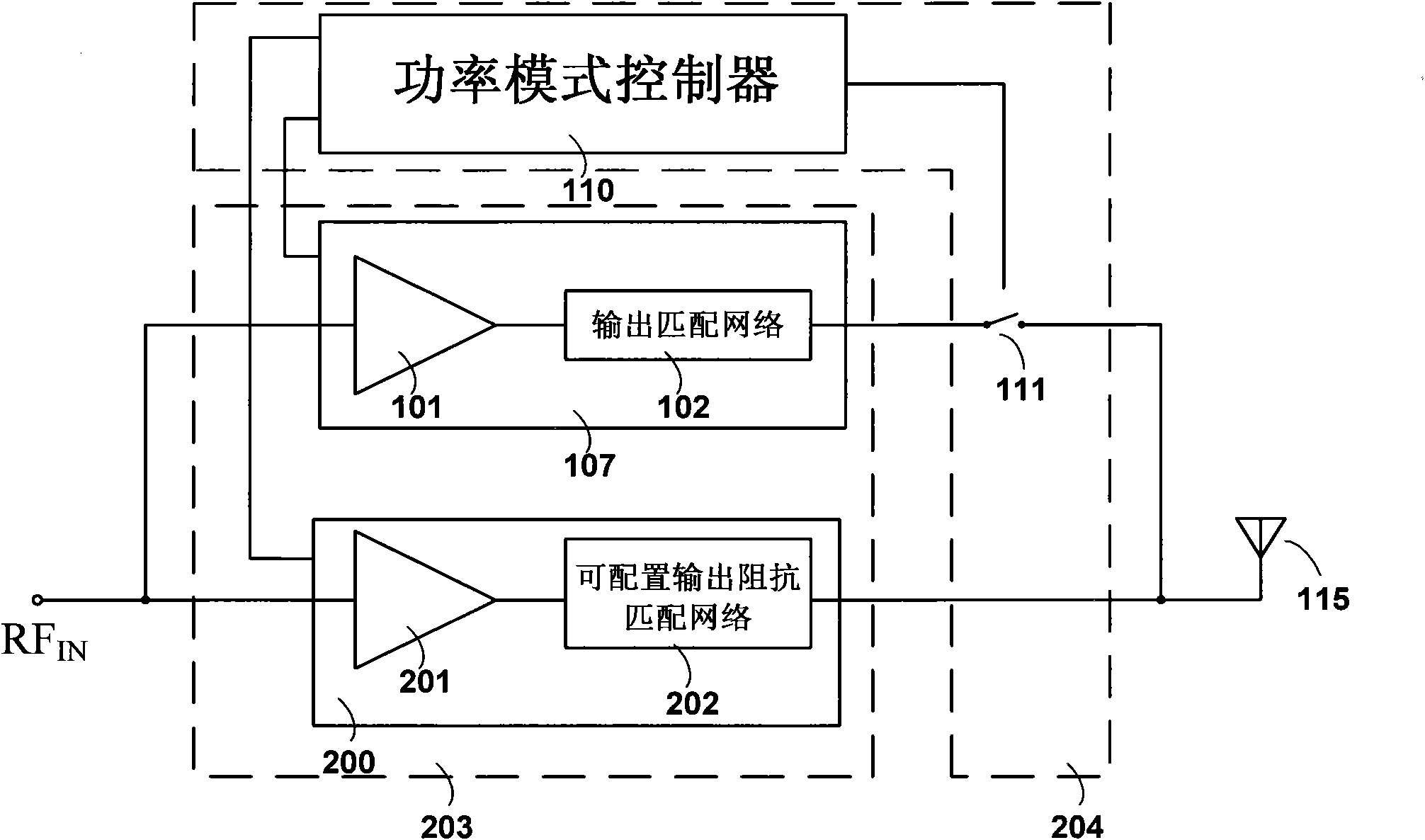
[0043] The structure of the first multi-power mode radio frequency transmitting front-end module proposed by the present invention is as follows: image 3 shown. The entire radio frequency transmitting front end is integrated into a single module, which includes a first chip 203 and a second chip 204 . The first chip 203 integrates a high power mode radio frequency power amplifier die 101 and its output matching network 102 and a configurable radio frequency power amplifier 200 with a configurable output impedance matching network 202, the configurable radio frequency power amplifier 200 includes a configurable output impedance The matching network 202 and the configurable radio frequency power amplifier die 201, the bias voltage of the configurable radio frequency power amplifier die 201 can be changed; the first chip 203 is usually manufactured by GaAs HBT process. The power mode controller 110 and the radio frequency switch 111 are integrated on the second chip 204 . The ...
Embodiment 3
[0046] The structure of the second multi-power mode radio frequency transmitting front-end module proposed by the present invention is as follows: Figure 4 shown. The entire radio frequency transmitting front end is integrated into a single module, which includes a third chip 205 and a fourth chip 206 . The high power mode radio frequency power amplifier die 101 and the configurable radio frequency power amplifier die 201 are integrated on the third chip 205; the third chip 205 is generally manufactured by GaAs HBT process. The fourth chip 206 integrates a power mode controller 110 , a radio frequency switch 111 , an output matching network 102 of a high power mode radio frequency power amplifier, and a configurable output impedance matching network 202 of a configurable radio frequency power amplifier 200 . The fourth chip is fabricated using a silicon-on-insulator (SOI) process. Because SOI is compatible with the traditional CMOS process on the one hand, it can be conveni...
PUM
| Property | Measurement | Unit |
|---|---|---|
| Resistivity | aaaaa | aaaaa |
Abstract
Description
Claims
Application Information