Supercharge Your Innovation With Domain-Expert AI Agents!

Internal memory interface circuit framework supporting multi-internal memory standard and implementation thereof on metal oxide semiconductor (MOS) process

A technology of circuit structure and process, applied in the fields of logic circuit coupling/interface, logic circuit connection/interface layout, information storage, etc. using field effect transistors, which can solve the problems of chip failure, sharp increase in area, and performance degradation.

Inactive Publication Date: 2010-12-29
合肥力杰半导体科技有限公司 +1
View PDF4 Cites 8 Cited by
  • Summary
  • Abstract
  • Description
  • Claims
  • Application Information

AI Technical Summary

Problems solved by technology

To support multiple interface standards, the easiest way is to put several different interfaces together, but this will not only increase the area dramatically, but also increase power consumption and reduce performance due to the increase in input and output loads
The increase of the area will lead to a series of problems, including the increase of cost, the decrease of yield rate, and the integration of chips becomes more complicated or even impossible.
Not only that, because different memory interface standards also use different I / O voltages, so different power supply networks need to be used, which will increase the cost of the chip and lead to potential chip failure, so the design of the multi-mode interface cannot be a simple overlay

Method used


Image

  • Internal memory interface circuit framework supporting multi-internal memory standard and implementation thereof on metal oxide semiconductor (MOS) process
  • Internal memory interface circuit framework supporting multi-internal memory standard and implementation thereof on metal oxide semiconductor (MOS) process
  • Internal memory interface circuit framework supporting multi-internal memory standard and implementation thereof on metal oxide semiconductor (MOS) process

Examples


Embodiment Construction

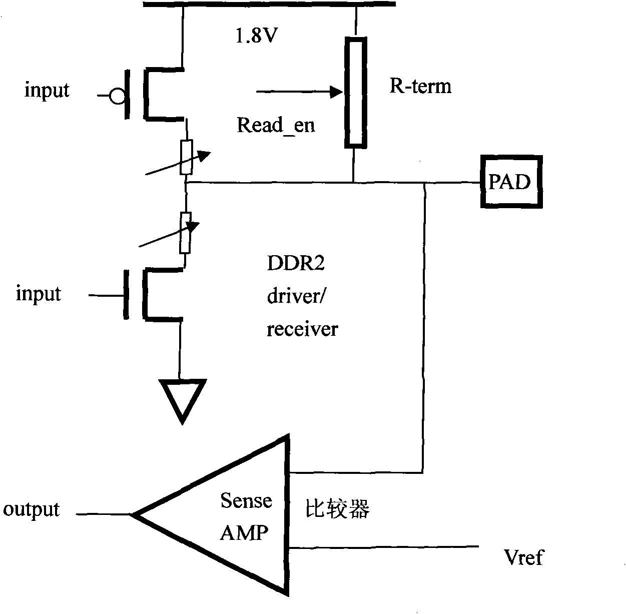
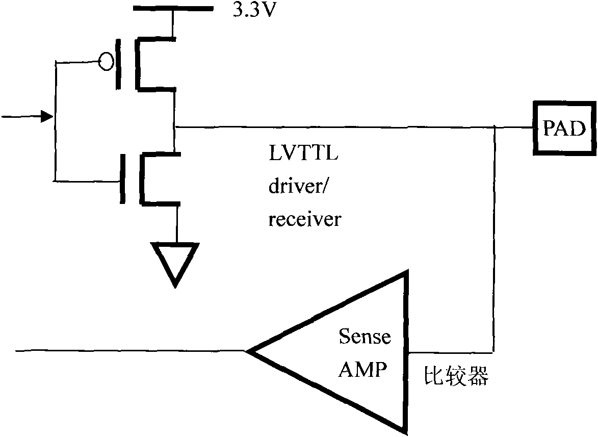
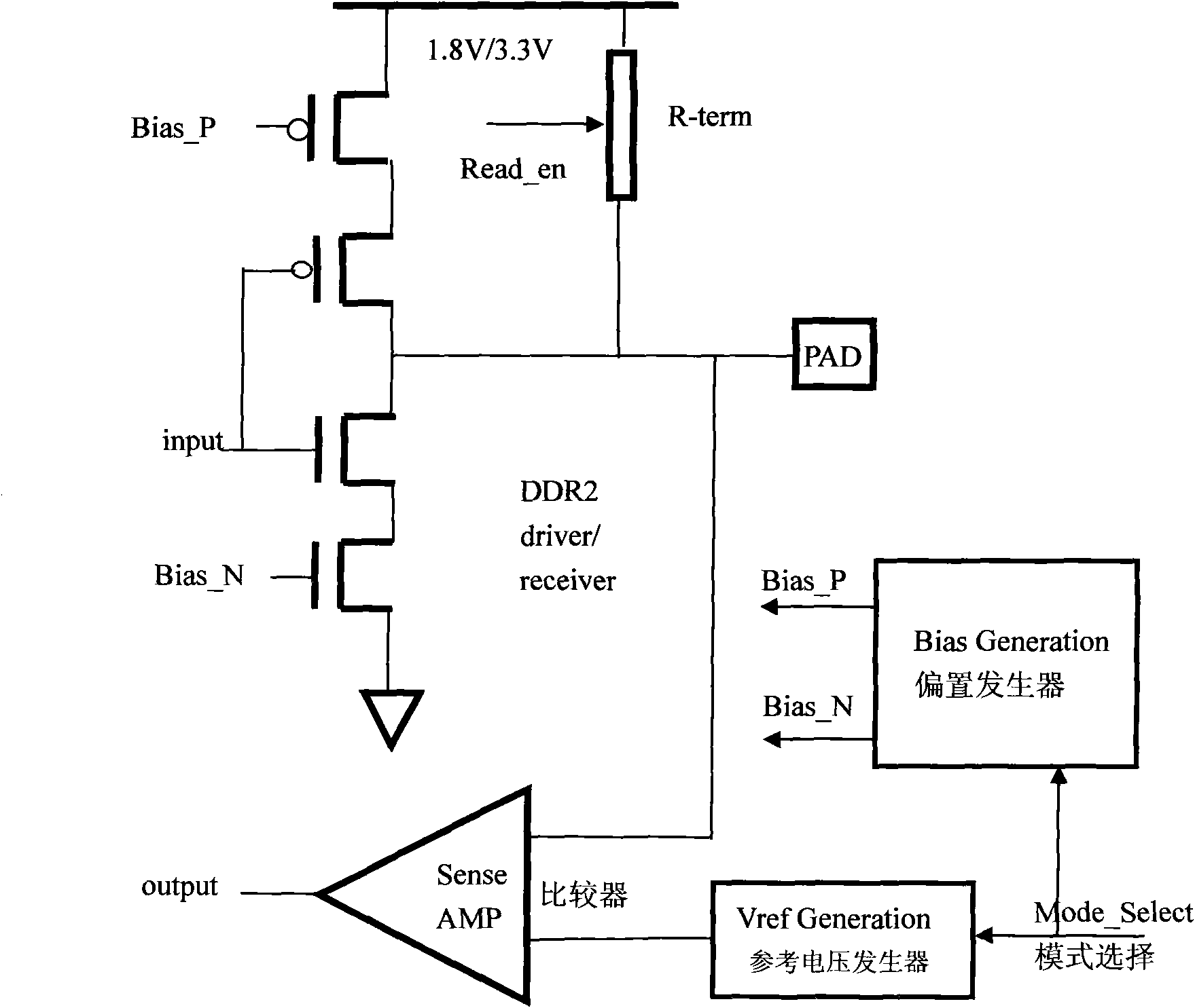
[0011] This patent is implemented in accordance with the content of the third article, and the interface circuit supporting DDR2 or DDR3 is modified. The specific implementation can be carried out according to Figure 4 , 5 , 6 instructions, so that the interface circuit to achieve the purpose of supporting 4 different memory standards. After the transformation is completed, select the power supply voltage according to the different memory standards supported. For example, if it is SDR SDRAM, use 3.3V power supply voltage, and if mobile SDRAM, DDR2, and mobile DDR use 1.8V voltage. A four-to-one selection circuit is added to the input and output ends of the interface, and the interface is controlled through the mode selection signal to make it work normally.

[0012] The area and power consumption of the memory interface described in this patent are increased by about 30% on the basis of only supporting DDR2 interface circuits, and the simple solution of stacking circuits of ...


PUM


Abstract

The invention belongs to the field of complementary metal oxide semiconductor (CMOS) integrated circuits and discloses hybrid multimode internal memory interface support technology for a CMOS integrated circuit apparatus. The technology can support four or more internal memory standards by only modifying a double data rate 2 (DDR2) or DDR3 supporting interface circuit and adding certain auxiliary circuits without remarkably increasing an area or power consumption. The technology is suitable for designing a central processing unit (CPU), a system on chip (SoC), an application specific integrated circuit (ASIC) and other application chips adopting internal memory interfaces so as to improve flexibility and compatibility. An implementation method described by the invention is applied to a 65-nanometer tape-out process for two times and is verified. Infringement of the invention can be generally judged by analyzing an implementation circuit or by a backward analysis method for dissecting and photographing the chip of the circuit under the condition that the circuit cannot be obtained. Institutes which may infringe include various field-containing and field-free chip design companies, research institutes, schools and the like.

Description

1. Technical field [0001] The patent of the invention belongs to the field of CMOS integrated circuits. It is aimed at memory interface related chips of CMOS integrated circuits, covering all memory standards, including SDR SDRAM.Mobile SDRAM, DDR / DDR2SDRAM, mobile SDRAM, DDR3 SDRAM. This patent is not limited to a certain integrated Circuit production process, which covers 0.35um, 0.25um, 0.18um, 0.13um, 90nm, 65nm, 45nm, 32nm and shrink processes related to these processes. This technology is applicable to the design of CPU, SoC, ASIC and other application chips using memory interface to improve their flexibility and compatibility. 2. Technical background [0002] With the continuous improvement of semiconductor manufacturing technology and the continuous improvement of chip design capabilities, the functions of various processors are also improving rapidly, and higher requirements are put forward for the capacity and speed of memory. Memory technology is also constantly ...

Claims


Application Information

Patent Timeline
IPC IPC(8): G11C7/10H03K19/0185G06F3/00
Inventor 陈峰王标夏先衡邰连梁刘清卫夏洪锋李广仁
Owner 合肥力杰半导体科技有限公司
Features
  • R&D
  • Intellectual Property
  • Life Sciences
  • Materials
  • Tech Scout
  • Unparalleled Data Quality
  • Higher Quality Content
  • 60% Fewer Hallucinations
Learn More