Method and device for digitizing an analog electrical signal and method for digitizing
An electrical signal and signal technology, applied in the direction of analog-to-digital converter, analog-to-digital conversion, electrical components, etc., can solve the problems of complex and laborious, inverse operation, difficult temperature compensation, etc.
- Summary
- Abstract
- Description
- Claims
- Application Information
AI Technical Summary
Problems solved by technology
Method used
Image

Examples
Embodiment Construction
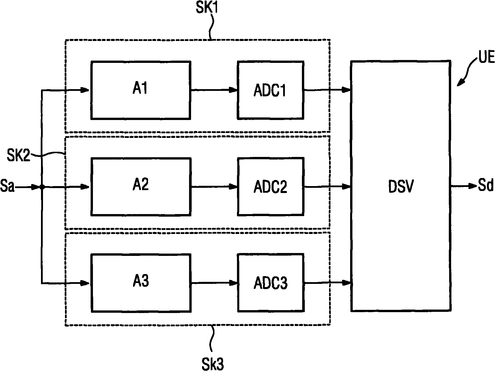
[0021] figure 1 A block diagram of a device for digitizing an analog electrical signal Sa is shown. The device has a plurality (here three) of sub-channels SK1 , SK2 , SK3 connected in parallel, to which the signal Sa is simultaneously applied. The signal Sa is then amplified in each subchannel SK1 , SK2 , SK3 (signal amplification section A1 , A2 , A3 ) before the signal is supplied to the input of the AD converter ADC1 , ADC2 , ADC3 . The output values of the AD converters ADC1 , ADC2 , ADC3 then enter a common digital signal processor DSV, which receives the values (receiver UE) and forms and outputs the total digital value Sd therefrom.
[0022] The AD converters ADC1 , ADC2 , ADC3 are here identical in each case in the exemplary embodiment (but it is also possible to use different AD converters in each sub-channel SK1 , SK2 , SK3 ).
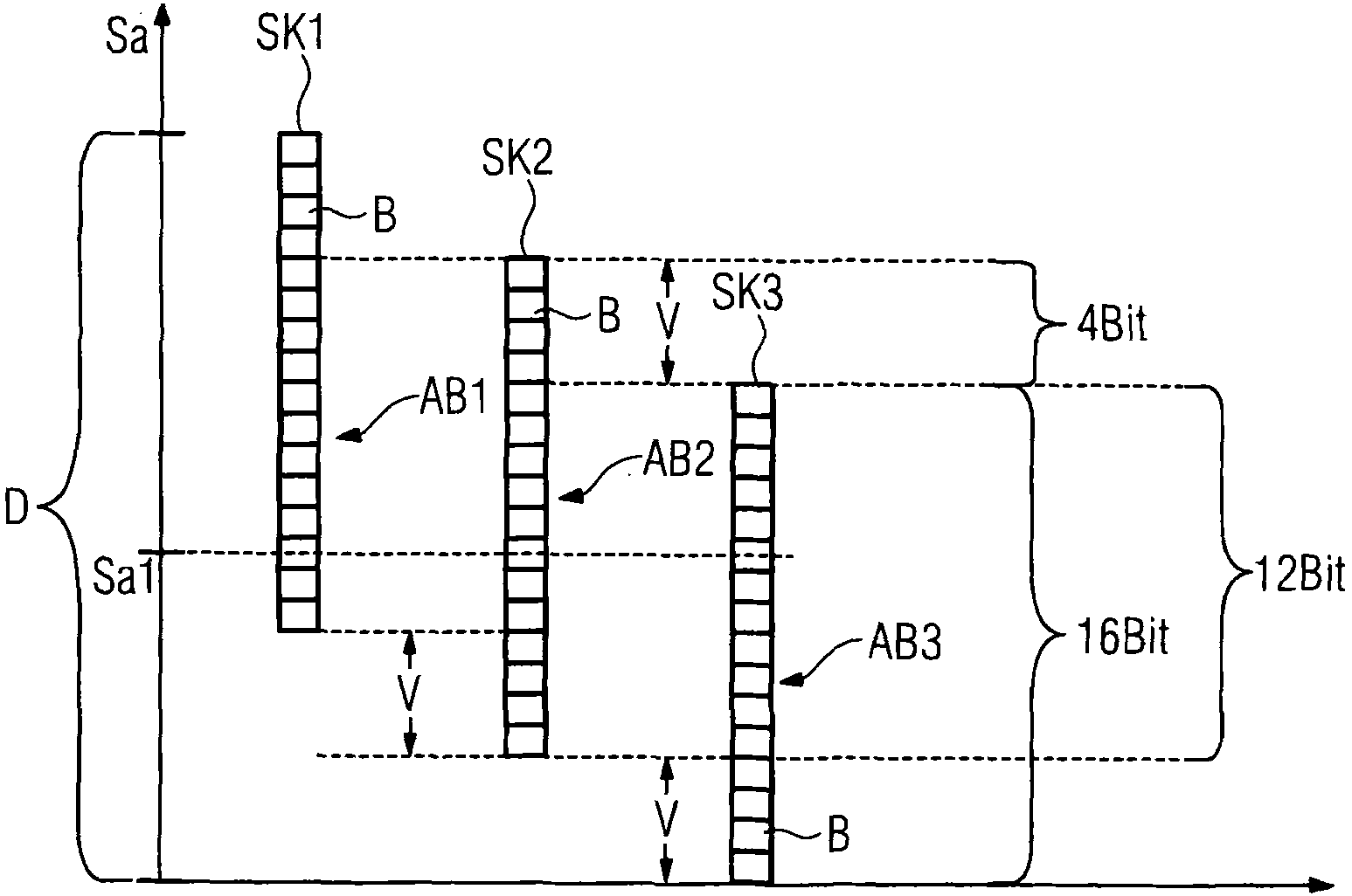
[0023] The amplitude of the signal Sa is within the total amplitude range (total dynamic range) D, and D is 24Bit. When the resoluti...
PUM
 Abstract
Description
Claims
Application Information
PatSnap Eureka turns technology decisions into work you can execute. Powered by our Innovation Knowledge Graph, it runs expert workflows across engineering, life sciences, materials and intellectual property. Get your review-ready output in minutes.


