Liquid crystal display panel and manufacturing method thereof

A technology of liquid crystal display panel and manufacturing method, which is applied in the direction of nonlinear optics, instruments, optics, etc., and can solve the problems of liquid crystal outflow, liquid crystal pollution of frame glue, holes in frame glue, etc., so as to save materials and costs, and prevent stretching damage or oily handwriting intrusion, the effect of eliminating pollution

Inactive Publication Date: 2011-02-16
AU OPTRONICS (SUZHOU) CORP LTD +1
View PDF4 Cites 2 Cited by
  • Summary
  • Abstract
  • Description
  • Claims
  • Application Information

AI Technical Summary

Problems solved by technology

[0003] However, the display panel 4 with the above structure is often accompanied by the following disadvantages: (1) Before the sealant 3 is hardened, the sealant will pollute the liquid crystal, causing various defects of the display panel 4, such as unevenness of the four colors of the display panel
(2) When heating and curing, due to the volatilization of the solvent in the frame glue, the frame glue will produce holes, causing the liquid crystal to flow out

Method used


Image

  • Liquid crystal display panel and manufacturing method thereof
  • Liquid crystal display panel and manufacturing method thereof
  • Liquid crystal display panel and manufacturing method thereof

Examples


Embodiment Construction

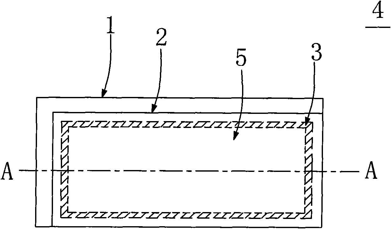
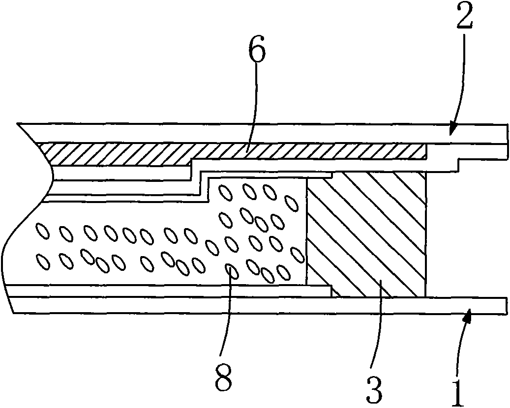
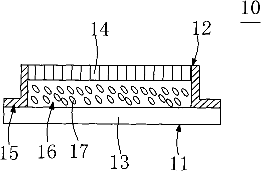
[0025] See image 3 , image 3 Shown is a schematic diagram of a liquid crystal display panel according to the present invention. The present invention provides a liquid crystal display panel 10 . The liquid crystal display panel 10 includes a first substrate 11 , a second substrate 12 and a liquid crystal layer 17 . Wherein, the first substrate 11 is a thin film transistor array substrate, and the second substrate 12 is a color filter substrate. The first substrate 11 has a first insulating substrate 13 , such as a glass substrate; the second substrate 12 has a second insulating substrate 14 made of plastic material. In addition, the first substrate 11 also includes scanning wires, data wires, thin film transistors, and pixel electrodes formed on the first insulating substrate 13 , and the second substrate 12 also includes black wires formed on the second insulating substrate 14 . Matrix, color layer, protective layer, transparent electrode (ITO) conductive film, etc. And...


PUM


Abstract

The invention discloses a liquid crystal display (LCD) panel and a manufacture method thereof. The LCD panel comprises a first substrate, a second substrate and a liquid crystal layer, wherein the first substrate is provided with a first insulating substrate; the second substrate is provided with a second insulating substrate prepared by a plastic material; an adsorption region is arranged on the periphery of the second insulating substrate, and is adhered to the first insulating substrate to ensure that the first substrate and the second substrate are combined and fixed to form an accommodating region; and the liquid crystal layer is accommodated in the accommodating region. The LCD panel and the manufacture method thereof can save the procedure of frame glue coating, and eliminate pollution, pores and other related adverse influences generated by using a frame coating.

Description

technical field [0001] The present invention relates to a liquid crystal display panel and a manufacturing method thereof, in particular to a liquid crystal display panel in which two substrates are fixed by vacuum adsorption and a manufacturing method of the liquid crystal display panel. Background technique [0002] See figure 1 and figure 2 , figure 1 Shown is a schematic diagram of a liquid crystal display panel in the prior art, figure 2 shown along figure 1 Schematic cross-sectional view of line AA. At present, in traditional liquid crystal display devices, the insulating substrates of the thin film transistor array (TFT) substrate 1 and the color filter (CF) substrate 2 are all made of glass substrates, and the CF substrate 2 and the TFT substrate 1 are bonded by a frame glue 3 to form a display. The panel 4 and the display area 5 of the display panel 4 are used for displaying images. The TFT substrate 1 mainly includes a glass substrate and scanning wiring, d...

Claims


Application Information

Patent Timeline
Patent Type & Authority Applications(China)
IPC IPC(8): G02F1/1335G02F1/1333
Inventor 田昕
Owner AU OPTRONICS (SUZHOU) CORP LTD
Why Eureka
Try Eureka