

Hardening structure touch panel and manufacturing method thereof
A touch panel and nameplate technology, applied in hardened structure touch panel and its manufacturing field, can solve the problems of rising, occupying manufacturing cost, and increasing the overall wiring width, so as to improve light transmittance, reduce thickness and weight , the effect of reducing thickness
- Summary
- Abstract
- Description
- Claims
- Application Information
AI Technical Summary
Problems solved by technology
Method used
Image

Examples
Embodiment 1
[0032] A method for manufacturing a touch panel with a hardened structure, comprising the following steps performed under dust-free and dry conditions;
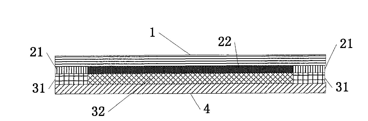
[0033] Step 1: printing an ink frame 31 on the transparent substrate layer 4;
[0034] Step 2: coating the surface of the transparent substrate layer 4 inside the ink frame 31 with a hardness enhancing liquid;
[0035] Step 3: forming a transparent hard coat layer 32 through the actinic hardness strengthening liquid, and the thickness of the transparent hard coat layer 32 is the same as that of the ink frame 31;
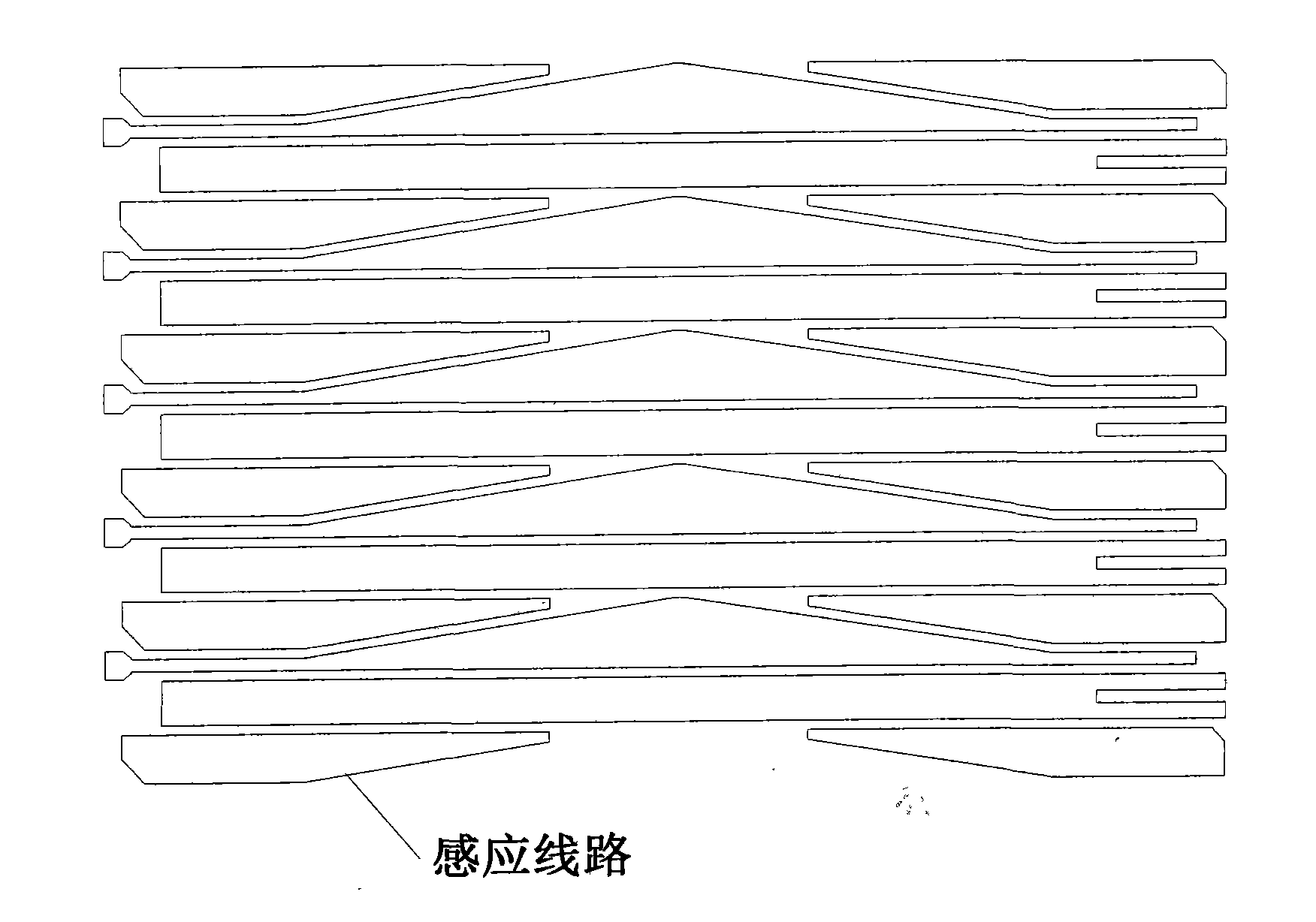
[0036] Step 4: The surface of the transparent hard coat layer 32 is coated with a transparent conductive layer, and the transparent conductive layer is laser cut to obtain the pattern sensing layer 22;
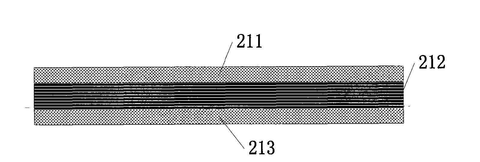
[0037] Step 5: Print the first silver line layer 211 on the ink frame 31 in step 3, and one end thereof is connected to the edge end of the pattern sensing layer 22, and the insulating ink layer 212 is formed by pr...
Embodiment 2
[0041] A method for manufacturing a touch panel with a hardened structure, comprising the following steps performed under dust-free and dry conditions;
[0042] Step 1: printing an ink frame 31 on the transparent substrate layer 4;
[0043] Step 2: coating the surface of the transparent substrate layer 4 inside the ink frame 31 with a hardness enhancing liquid;
[0044] Step 3: forming a transparent hard coat layer 32 through the actinic hardness strengthening liquid, and the thickness of the transparent hard coat layer 32 is the same as that of the ink frame 31;
[0045] Step 4: plate a transparent conductive layer on the surface of the transparent hard coat layer 32, and etch the transparent conductive layer to obtain the pattern sensing layer 22;
[0046] Step 5: Print the first silver line layer 211 on the ink frame 31 in step 3, and one end thereof is connected to the edge end of the pattern sensing layer 22, and the insulating ink layer 212 is formed by printing two lay...
Embodiment 3
[0050] A method for manufacturing a touch panel with a hardened structure, comprising the following steps performed under dust-free and dry conditions;
[0051] Step 1: printing an ink frame 31 on the transparent substrate layer 4;
[0052] Step 2: coating the surface of the transparent substrate layer 4 inside the ink frame 31 with a hardness enhancing liquid;
[0053] Step 3: forming a transparent hard coat 32 with a thermal hardness enhancing liquid, and the thickness of the transparent hard coat 32 is the same as that of the ink frame 31;
[0054] Step 4: The surface of the transparent hard coat layer 32 is coated with a transparent conductive layer, and the transparent conductive layer is laser cut to obtain the pattern sensing layer 22;
[0055] Step 5: Print the first silver line layer 211 on the ink frame 31 in step 3, and one end thereof is connected to the edge end of the pattern sensing layer 22, and the insulating ink layer 212 is formed by printing two layers of ...
PUM
| Property | Measurement | Unit |
|---|---|---|
| Thickness | aaaaa | aaaaa |
| Thickness | aaaaa | aaaaa |
| Thickness | aaaaa | aaaaa |
Abstract
Description
Claims
Application Information