Steady-state thermal analysis method of stack type three-dimensional FPGA (Field Programmable Gate Array) chip

A thermal analysis, stacked technology, used in special data processing applications, instruments, electrical digital data processing, etc.

Inactive Publication Date: 2011-02-16
FUDAN UNIV
View PDF1 Cites 19 Cited by
  • Summary
  • Abstract
  • Description
  • Claims
  • Application Information

AI Technical Summary

Problems solved by technology

[0008] Thermal analysis models for FPGAs, especially 3D FPGAs, are emerging and have not been studied much in the past

Method used


Image

  • Steady-state thermal analysis method of stack type three-dimensional FPGA (Field Programmable Gate Array) chip
  • Steady-state thermal analysis method of stack type three-dimensional FPGA (Field Programmable Gate Array) chip
  • Steady-state thermal analysis method of stack type three-dimensional FPGA (Field Programmable Gate Array) chip

Examples


Embodiment Construction

[0091] The solutions of the present invention will be further described below in conjunction with the accompanying drawings and specific embodiments.

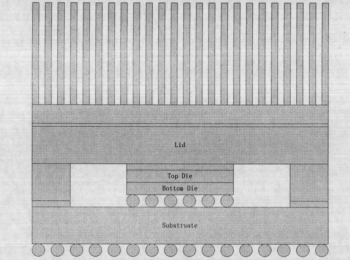
[0092] Figure 15 It is a stacked chip design including two FPGA chips. B represents the contact point between chip 1 and chip 2, and X represents the internal point of chip 1. Define B’ and Y in the same way. It can be seen that B and B' represent the same point in this stacked chip structure, but in order to simplify the analysis, we regard B and B' as different points, and B and B' are connected by a one-dimensional superconductor, we This hypothetical structure of high thermal conductivity is called a virtual element.

[0093] Figure 16 is a flow chart of the stacked three-dimensional FPGA chip thermal analysis algorithm, [K i ] is the heat conduction matrix of chip i, in the following we will analyze the structure of the matrix [K] in detail, and how the preprocessing matrix is ​​established.

[0094] The thermal cond...


PUM


Abstract

The invention belongs to the technical field of electronic design automation, in particular to a steady-state thermal analysis method of a stack type three-dimensional FPGA (Field Programmable Gate Array) chip. The method only needs a packaging thermal model on a minimum boundary to accurately estimate the temperature and the power consumption on the chip by adopting a minimum boundary method, and once the temperature can be accurately calculated, the method can reduce the temperature on the basis of a traditional mechanism. The thermal analysis method ensures that the thermal analysis accuracy of the stack type three-dimensional FPGA chip is higher, and the analysis process and the packaging model are simplified. Based on the thermal model of the stack type three-dimensional FPGA chip, a finite element method is used as a basic thermal analysis algorithm, the invention provides an accurate and effective algorithm for steady-state thermal analysis of the stack type three-dimensional FPGA chip, and due to convenient realization, the steady-state thermal analysis method can be rapidly applied to the present design process.

Description

technical field [0001] The invention belongs to the technical field of EDA (Electronic Design Automation, electronic design automation), and in particular relates to a thermal analysis model and a steady-state thermal analysis method of a stacked three-dimensional FPGA chip. Background technique [0002] With the advancement of semiconductor process technology, power consumption has become an important factor that must be considered in the chip design process. Compared with ASIC (Applied System Integrated Circuit, application-specific system integrated circuit), FPGA (Field Programmable Gate Array, Field Programmable Gate Array) requires a large number of additional programmable switches in order to realize its programmable flexibility. Therefore, generally speaking, for the same application, FPGA consumes several times more power consumption than ordinary ASIC. For example, to implement an eight-bit adder as well, the difference in power consumption between FPGA and ASIC i...

Claims


Application Information

Patent Timeline
Patent Type & Authority Applications(China)
IPC IPC(8): G06F17/50
Inventor 余慧吴昊陈更生孙峥
Owner FUDAN UNIV
Why Eureka
Try Eureka