Transistor structure with etch stop layer and manufacturing method thereof

An etch stop layer and etch stop technology, which is applied in transistors, semiconductor/solid-state device manufacturing, semiconductor devices, etc., can solve the problem of uneven electrical properties of transistors and achieve good reliability

Active Publication Date: 2011-02-16
AU OPTRONICS CORP
View PDF3 Cites 6 Cited by
  • Summary
  • Abstract
  • Description
  • Claims
  • Application Information

AI Technical Summary

Problems solved by technology

[0004] The technical problem to be solved by the present invention is to propose a transistor structure with an etch stop layer and its manufacturing method to improve the problem of uneven electrical properties of existing transistors

Method used


Image

  • Transistor structure with etch stop layer and manufacturing method thereof
  • Transistor structure with etch stop layer and manufacturing method thereof
  • Transistor structure with etch stop layer and manufacturing method thereof

Examples


Embodiment 1

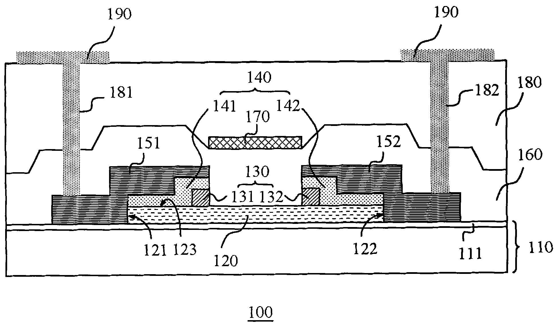
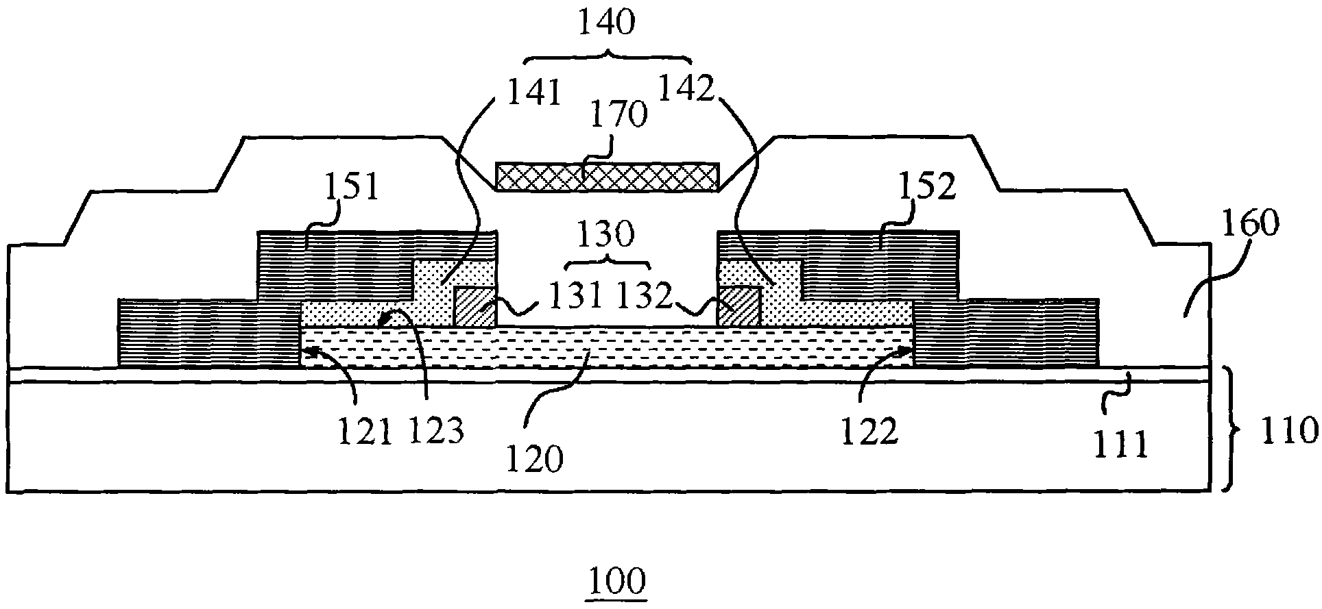
[0053] Next, with the reference Figure 2A , 2B , respectively depict schematic diagrams of Embodiments 1 and 2 of the main characteristic structure of the transistor of the present invention. Such as Figure 2A In the first embodiment shown, the first part 131 of the etch stop structure 130 is sandwiched between the first ohmic contact region 141 and the crystalline semiconductor layer 120, and the second part 132 of the etch stop structure 130 is sandwiched between the first ohmic contact region 141 and the second crystalline semiconductor layer 120. Directly below the two ohmic contact regions 142 and between the crystalline semiconductor layer 120 , and the first portion 131 and the second portion 132 of the etch stop structure 130 are not in contact. therefore, figure 1 In the transistor structure 100 , the etch stop structure 130 exposes the partially crystalline semiconductor layer 120 .

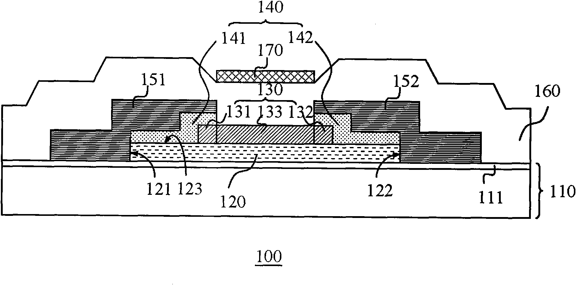
[0054] Also, if Figure 2B In the second embodiment shown, except for the fi...


PUM


Abstract

The invention discloses a transistor structure with an etch stop layer and a manufacturing method thereof. The transistor structure of the invention is at least composed of a substrate, a crystallized semiconductor layer, an etch stop structure, an ohmic contact layer, a resource electrode, a drain electrode, a grid electrode insulating layer and a grid electrode. The manufacture method of the invention can simultaneously pattern the ohmic contact layer and the crystallized semiconductor layer by the same photomask or can simultaneously pattern the ohmic contact layer and an electrode layer by the other identical photomask.

Description

technical field [0001] The invention relates to a transistor structure, in particular to a thin film transistor structure with an etching stop layer. Background technique [0002] In the existing top gate structure (element) of thin film transistors, it has been widely used in flat-panel display devices. The top gate means that the gate is arranged above the semiconductor stack layer, and the semiconductor stack layer is made of polysilicon layer and an ohmic contact layer, that is, a polysilicon layer is formed first, and then an ohmic contact layer is formed on the polysilicon layer, and the ohmic contact layer has an N+ region and a P+ region. However, in the general top gate (top gate) transistor element process, when etching the ohmic contact layer, that is, when etching the N+ region and the P+ region, it is easy to etch the polysilicon layer directly below the gate and its vicinity, resulting in The front channel of the polysilicon layer (also called the active layer...

Claims


Application Information

Patent Timeline
Patent Type & Authority Applications(China)
IPC IPC(8): H01L21/336H01L29/786H01L21/28H01L29/06H01L29/45H01L29/41
Inventor 胡晋玮庄景桑陈佳榆
Owner AU OPTRONICS CORP
Why Eureka
Try Eureka