Four-junction semiconductor solar photovoltaic cell chip
A photovoltaic cell and semiconductor technology, applied in the field of four-junction semiconductor solar photovoltaic cell chip structure, can solve the problems of energy absorption and utilization, low photoelectric conversion efficiency of solar cell chips, etc.
- Summary
- Abstract
- Description
- Claims
- Application Information
AI Technical Summary
Problems solved by technology
Method used
Image
Examples
Embodiment Construction
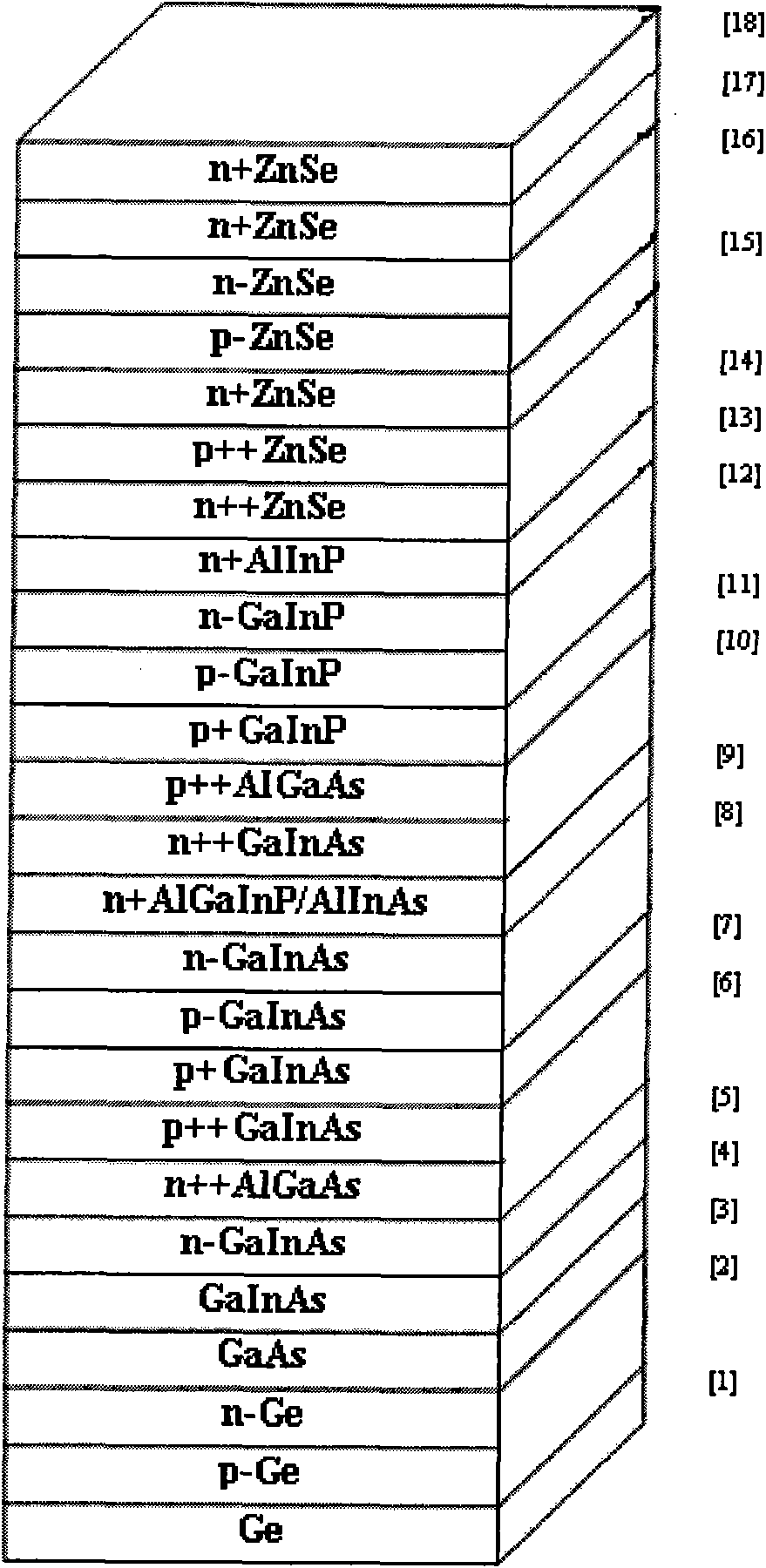
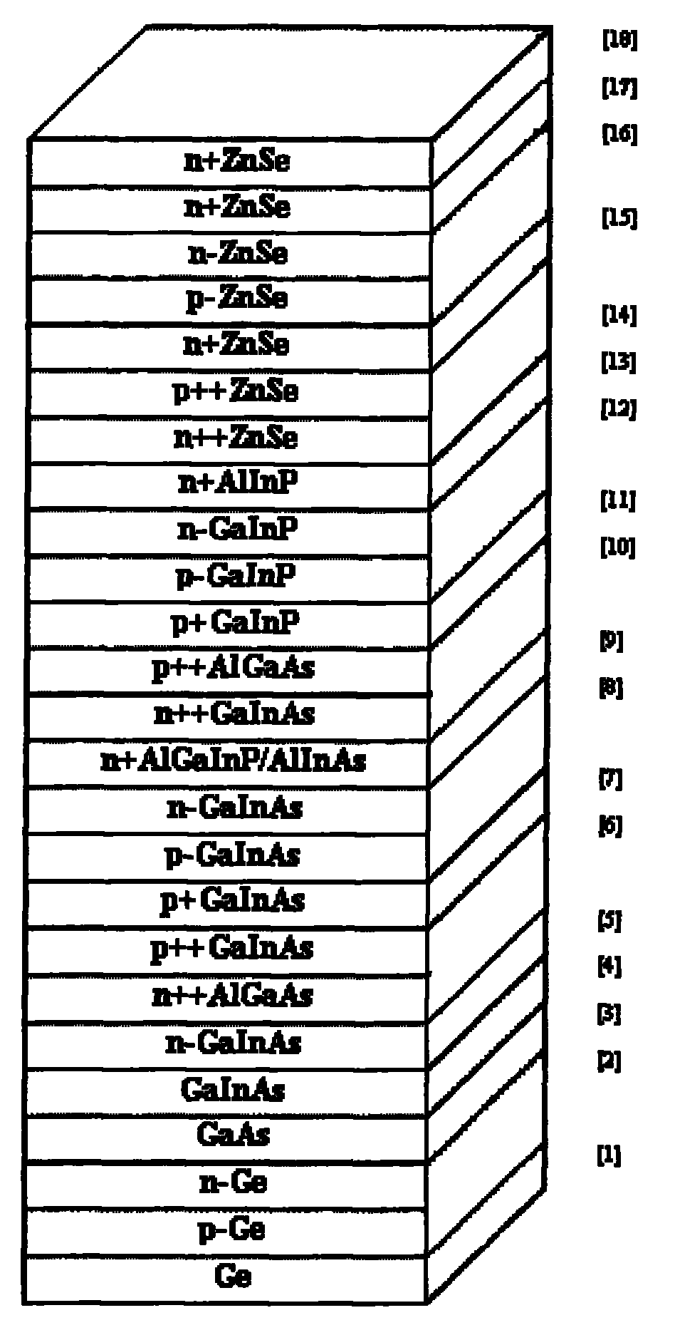
[0011] In order to further illustrate the structure and features of the present invention, the present invention will be further described below in conjunction with the embodiments and accompanying drawings. Such as figure 1 As shown, a four-junction semiconductor solar photovoltaic cell chip adopts the metal organic chemical vapor deposition (MOCVD) method, and the bottom cells (p-Ge, n-Ge) 2 are sequentially grown on the germanium (Ge) single wafer 1 as the substrate, forming Core layer (GaAs) 3, buffer layer (GaInAs) 4, barrier layer (n-GaInAs) 5, tunnel junction (n++AlGaAs, p++GaInAs) 6, barrier layer (p+GaInAs) 7, the Two-junction cell (p-GaInAs, n-GaInAs) 8, window layer (n+AlGaInP / AlInAs) 9, second tunnel junction (n++GaInAs, p++AlGaAs) 10, second barrier layer (p+ GaInP) 11, the third junction cell (p-GaInP, n-GaInP) 12, the second window layer (n+AlInP) 13, the third tunnel junction (n++ZnSe, p++ZnSe) 14, the third potential Barrier layer (n+ZnSe) 15, top cell (p-Zn...
PUM
 Abstract
Description
Claims
Application Information

