Surface plasma excitation method for chip-integrated metal nanowire

A technology of surface plasmons and metal nanowires, applied in light guides, optics, instruments, etc., can solve problems such as the inability to achieve chip integration, and achieve the effect of improving integration

Inactive Publication Date: 2011-03-16
ZHEJIANG UNIV
View PDF0 Cites 8 Cited by
  • Summary
  • Abstract
  • Description
  • Claims
  • Application Information

AI Technical Summary

Problems solved by technology

Traditional methods include prism total reflection coupling or objective lens focusing coupling based on the Kretschmann device. The disadvantage of these methods...

Method used


Image

  • Surface plasma excitation method for chip-integrated metal nanowire
  • Surface plasma excitation method for chip-integrated metal nanowire
  • Surface plasma excitation method for chip-integrated metal nanowire

Examples


Embodiment Construction

[0011] The present invention will be further described below in conjunction with the accompanying drawings and examples, and the purpose and effect of the present invention will become more obvious.

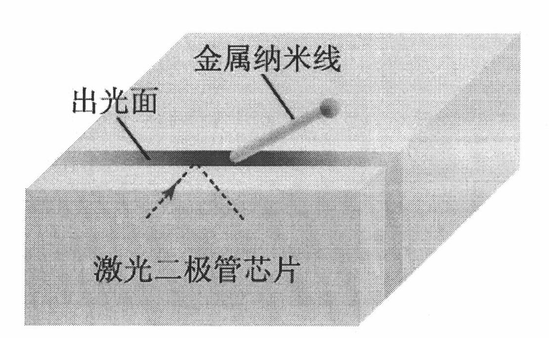
[0012] Such as figure 1 As shown, in the present invention, one end of the metal nanowire is placed on the light-emitting surface of the laser diode chip to excite the transmission of surface plasmons in the metal nanowire, and at the other end of the metal nanowire, the surface plasmon is coupled into free space light emission come out.

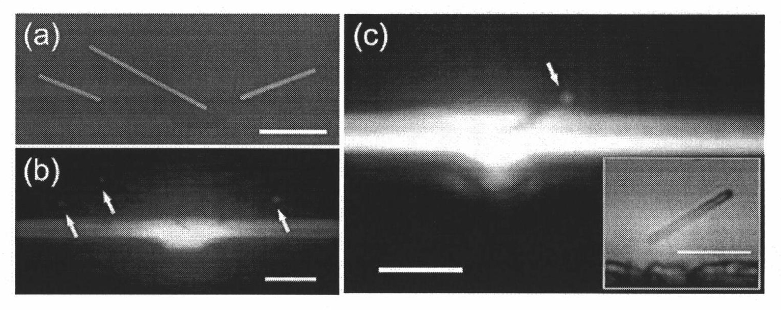
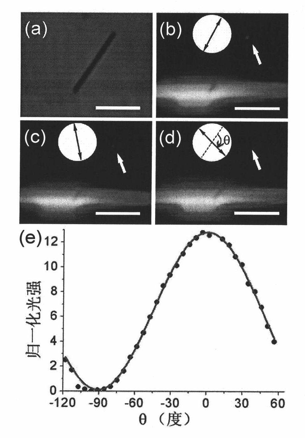
[0013] The diameter of the metal nanowire is 50-1000nm. Said laser diode is a general commercial laser diode with a wavelength of 400-2000nm. Such as figure 2 The laser diode used in (b) is the DL-3147-065 type red laser diode (center wavelength about 650nm) of Japan Sanyo Company, figure 2 (c) uses the RLD78NZH1 type infrared laser diode (center wavelength of about 785nm) of Rohm Company. The structure can be multiple or single nanowire...


PUM

PropertyMeasurementUnit
Diameteraaaaaaaaaa
Center wavelengthaaaaaaaaaa

Abstract

The invention discloses a surface plasma excitation method for chip-integrated metal nanowire, which comprises the following steps: a metal nanowire is arranged on a light emitting surface of a diode chip, and the plasma on an excitation surface is transmitted in the metal nanowires. In the excitation method of the invention, a light source and a plasma waveguide are integrated on the chip directly, thus omitting lens, prismas and other coupling devices in the conventional excitation method of the surface plasma; and linearly polarized light is output by the metal nanowire in the structure, and light intensity output can be adjusted by adjusting direction of the nanowire.

Description

technical field [0001] The invention relates to a surface plasmon excitation method, in particular to a chip-integrated excitation method of a light source and a surface plasmon waveguide. Background technique [0002] In the field of nanometers, metal nanowires have broad application prospects in the manufacture of electronics, photonics, and sensor devices. In recent years, with the improvement of the preparation process of metal nanowires, relatively low loss metal nanowires have been prepared and applied to the fabrication of surface plasmon-based Fabry-Perot optical resonators and the study of surface-enhanced Raman phenomena. However, how to realize the efficient coupling of light from the light source to the metal nanowires is still a practical problem that needs to be solved urgently. Traditional methods include prism total reflection coupling or objective lens focusing coupling based on Kretschmann devices. The disadvantage of these methods is that they use large-v...

Claims


Application Information

Patent Timeline
IPC IPC(8): G02B6/122G02B6/10
Inventor 童利民马哲张奚宁郭欣杨青马耀光
Owner ZHEJIANG UNIV
Why Eureka
Try Eureka