GaAs HBT high-gain broadband linear transconductance unit circuit

A transconductance unit, high gain technology, applied in logic circuits, improved amplifiers to reduce nonlinear distortion, electrical components, etc., can solve problems such as large DC voltage drop, achieve wide operating bandwidth, excellent linearity, and solve high gain. The contradictory effect of requirements and transistor saturation

Active Publication Date: 2011-03-23
INST OF MICROELECTRONICS CHINESE ACAD OF SCI
View PDF0 Cites 15 Cited by
  • Summary
  • Abstract
  • Description
  • Claims
  • Application Information

AI Technical Summary

Problems solved by technology

In addition, in order to provide high gain, according to the gain calculation formula A V =-g m · R L (where A V is the voltage gain of the transconductance circuit, g m is the transconductance, R L is

Method used


Image

  • GaAs HBT high-gain broadband linear transconductance unit circuit
  • GaAs HBT high-gain broadband linear transconductance unit circuit
  • GaAs HBT high-gain broadband linear transconductance unit circuit

Examples


Embodiment Construction

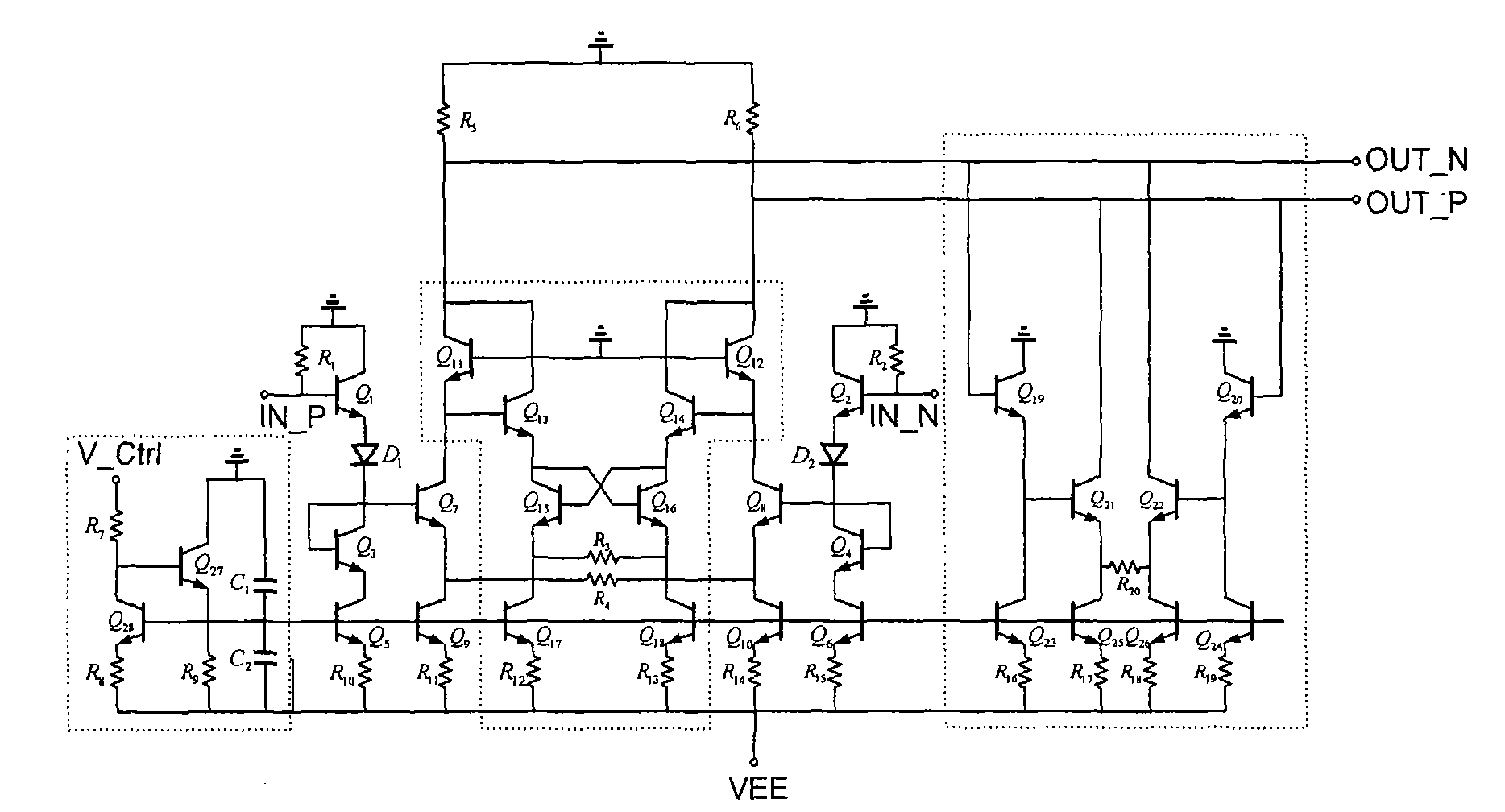
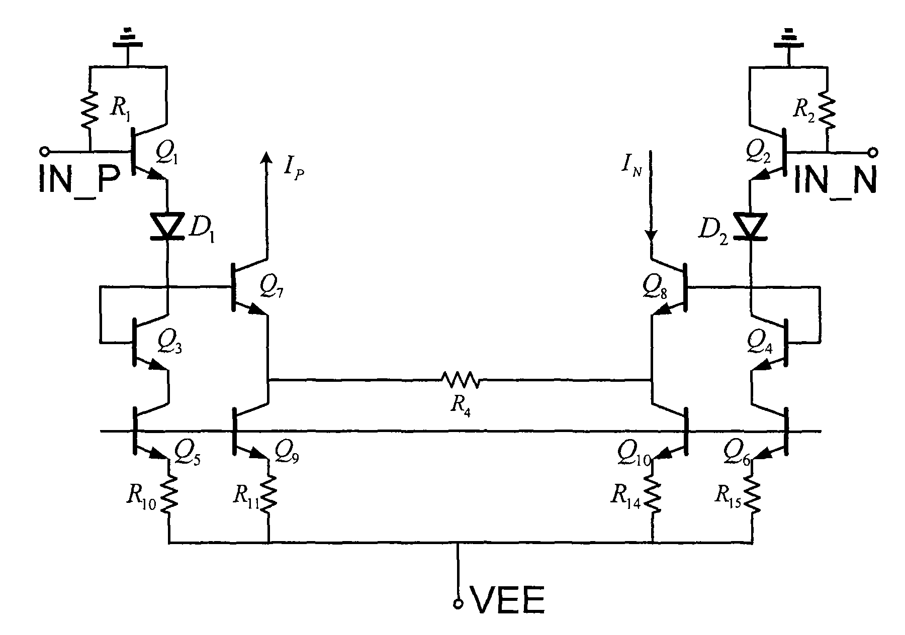
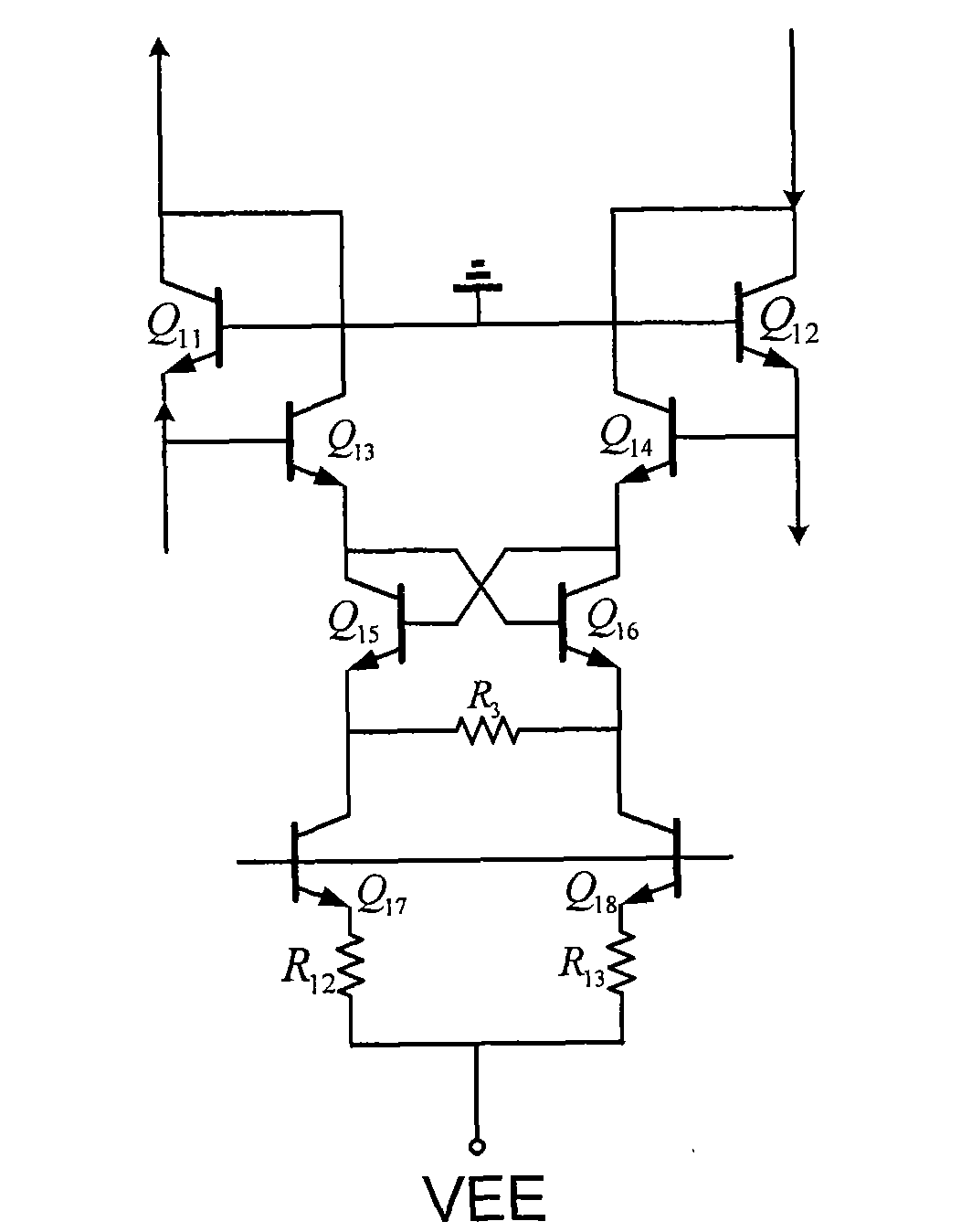
[0025] In order to make the object, technical solution and advantages of the present invention clearer, the present invention will be described in further detail below in conjunction with specific embodiments and with reference to the accompanying drawings. It should be noted that the circuit provided by the present invention is a fully differential structure, and all symmetrical HBT transistor devices and passive devices are completely matched; the upper rail of the power supply of the circuit is V CC =0V, the lower rail is V EE =-5.1V, so that the circuit can be compatible with emitter-coupled logic (ECL) digital circuits.

[0026] This GaAs HBT high-gain broadband linear transconductance unit circuit provided by the present invention adds a linearization subcircuit and a negative resistance subcircuit on the basis of the GaAs HBT basic transconductance circuit to improve the linearity and gain.

[0027] The GaAs HBT high-gain broadband linear transconductance unit circuit...


PUM


Abstract

The invention discloses a GaAs HBT high-gain broadband linear transconductance unit circuit comprising an input stage subcircuit, a basic transconductance subcircuit, a linear subcircuit, a negative resistance subcircuit and a mirror current source subcircuit, wherein the input stage subcircuit is used for level shift of input differential voltages IN_P and IN_N and conducts shifted signals into the basic transconductance subcircuit; the basic transconductance subcircuit is used for converting the input differential voltage signals into differential current signals; the linear subcircuit is used for improving the linearity of the basic transconductance subcircuit; the negative resistance subcircuit is used for improving the gain of the transconductance circuit; and the mirror current source subcircuit is used for providing bias current for the rest circuits. The circuit is designed and manufactured by a GaAs HBT technology and has wide operation bandwidth; the adopted linear subcircuit can effectively complement the nonlinearity of the circuit and provides excellent linearity; and the negative resistance subcircuit is adopted to effectively solve the conflict between the high-gainrequirement of circuits and transistor saturation and improves high-gain performance.

Description

technical field [0001] The present invention relates to the field of semiconductor device and integrated circuit design, in particular to a high-gain broadband linear transconductance unit designed by adopting gallium arsenide heterojunction bipolar transistor (GaAs HBT) technology to convert input differential voltage into differential output current circuit. Background technique [0002] Because of its excellent high-frequency and breakdown performance, GaAs HBT has become one of the best choices for designing and manufacturing radio frequency circuits and ultra-high-speed digital-analog hybrid circuits. Integrated circuits designed and manufactured using GaAs HBT technology have higher operating frequency and wider bandwidth, and have good device matching performance, and are suitable for large-scale digital-analog hybrid integrated circuits. The transconductance unit circuit is used to convert the input voltage signal into a current signal output, and is usually used in...

Claims


Application Information

Patent Timeline
IPC IPC(8): H03F1/32H03F3/45H03K19/018
Inventor 陈高鹏吴旦昱金智武锦刘新宇
Owner INST OF MICROELECTRONICS CHINESE ACAD OF SCI
Why Eureka
Try Eureka