Silicon-based active organic light emitting diode (OLED) display pixel circuit

A technology of light-emitting diodes and pixel circuits, applied to static indicators, instruments, etc., can solve problems such as gate-source voltage changes, OLED drive current glitches, production cost effects, etc., to achieve the effect of ensuring control and ensuring accuracy

Inactive Publication Date: 2011-03-30
NANKAI UNIV
View PDF3 Cites 51 Cited by
  • Summary
  • Abstract
  • Description
  • Claims
  • Application Information

AI Technical Summary

Problems solved by technology

Third, affected by the production cost, the pixel area of ​​silicon-based AMOLED is limited
When V COM When switching from high to low, the voltage of the drain terminal of M1 (connected to the OLED) drops, and at

Method used


Image

  • Silicon-based active organic light emitting diode (OLED) display pixel circuit
  • Silicon-based active organic light emitting diode (OLED) display pixel circuit
  • Silicon-based active organic light emitting diode (OLED) display pixel circuit

Examples


Embodiment 1

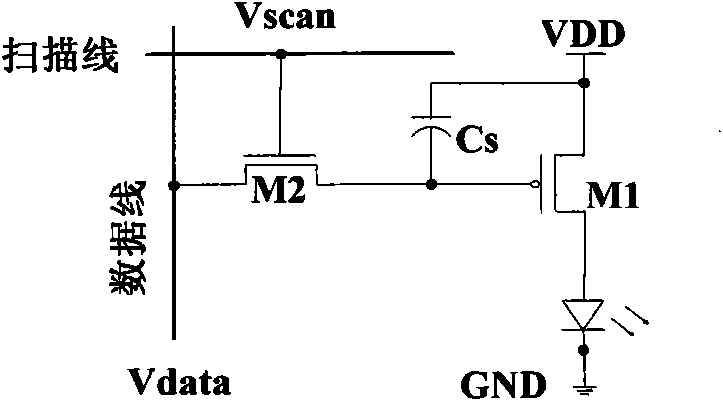
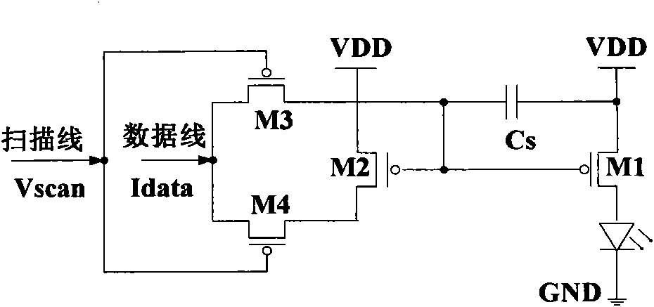
[0044] to improve Figure 4 The performance of the classic 2T1C circuit in AC application, the present invention proposes an improved 3T1C (3 transistors and a storage capacitor) voltage control pixel circuit, such as Figure 6 shown. and Figure 4 Compared with the circuit, this circuit only adds a switch tube M3 between the drive tube M1 and the OLED, and its gate is connected to the common cathode voltage V COM connected. The driving timing of the circuit is shown in the figure. Also during programming, Vscan and V COM is high level, the switch M2 is turned on, the storage capacitor is charged and the data voltage Vdata is stored. At this time, the OLED is in the reverse bias state, M1 and M3 are turned off, and no current flows; then enters the light-emitting stage, Vscan and V COM Change to low level, M2 is turned off, switch M3 is turned on, the data voltage Vdata stored on the storage capacitor makes M1 turn on, the OLED is forward-biased, and the driving current pr...

Embodiment 2、3T1

[0050] Embodiment 2, Further improvement scheme of 3T1C pixel circuit

[0051] Due to the small size of silicon-based AMOLED pixels, the driving current of the corresponding OLED area is very small, for example, the OLED current density is 40mA / cm 2 , then the drive current required for a 20μm×20μm pixel area is 20μm×20μm×40mA / cm 2 , ie 0.16µA. Even if the smallest size MOS tube is used, its current will still exceed the OLED current, unless the length of the MOS channel is lengthened as much as possible, which in turn contradicts the requirement of a smaller pixel area of ​​the silicon-based AMOLED. Therefore, the present invention proposes another pixel circuit to further reduce the driving current on the basis of the previous circuit. The circuit structure and working sequence are as follows: Figure 10 shown. In the figure, the storage capacitor is no longer fixedly connected to VDD, but is connected to the reference voltage VCH or VCL through a selection switch, where...


PUM


Abstract

The invention relates to a silicon-based active organic light emitting diode (OLED) display pixel circuit. On the basis of alternating-current driving of the classical 2T1C circuit, the invention provides an improved 3T1C voltage control pixel circuit which is characterized in that a switching tube M3 is additionally arranged between a driving tube M1 of a primary circuit and an OLED, and the grid electrode of the switching tube M3 is connected with the common cathode voltage VCOM. The current burrs appearing in the existing circuit can be effectively inhibited by reasonably adjusting the W/L ratio of the tube M1 and the tube M3. In addition, a time ratio gray scale method is used by the invention for driving the pixel circuit, thereby effectively realizing the gray scale display. The invention has the advantage that the gray scale display can be realized easily by controlling the time of the light-emitting stage; and simultaneously, the application of the alternating-current driving mode can provide a certain degree of electrical compensation for the degradation of OLED materials, and the additional arrangement of the tube M3 can further ensure the accuracy of the driving current, thereby ensuring the control of the gray scale display.

Description

【Technical field】: [0001] The invention belongs to the technical field of organic light emitting diode displays, in particular to a silicon-based active organic light emitting diode display pixel circuit. 【Background technique】: [0002] Silicon-based active organic light-emitting diode (OLED) display and its pixel circuit characteristics [0003] Silicon-based active organic light-emitting diode (AMOLED) display, as a new micro-display technology, fully combines the advantages of OLED and CMOS technology, and has unique advantages in the field of near-eye display. First of all, OLED is a self-luminous device, no backlight is needed, and optical accessories such as polarizers, beam splitters, and astigmatism screens required for the backlight of the corresponding liquid crystal microdisplay can be omitted; at the same time, OLED only emits light when needed. For video display , the average display brightness is 25% of the brightness when the screen is in full white display,...

Claims


Application Information

Patent Timeline
IPC IPC(8): G09G3/32G09G3/3233
Inventor 刘艳艳耿卫东代永平
Owner NANKAI UNIV
Why Eureka
Try Eureka