Method for fabricating circuit substrate assembly and power electronics module
A technology for circuit substrates and insulating substrates, applied in printed circuit parts, circuits, printed circuits, etc., can solve the problems of low thermal conductivity of ceramics, low thermal conductivity of metals, low mechanical bending load capacity, etc.
- Summary
- Abstract
- Description
- Claims
- Application Information
AI Technical Summary
Problems solved by technology
Method used
Image
Examples
Embodiment Construction
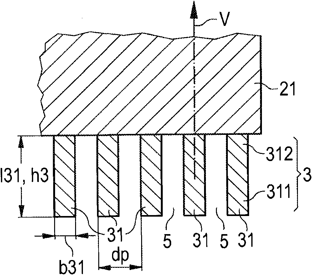
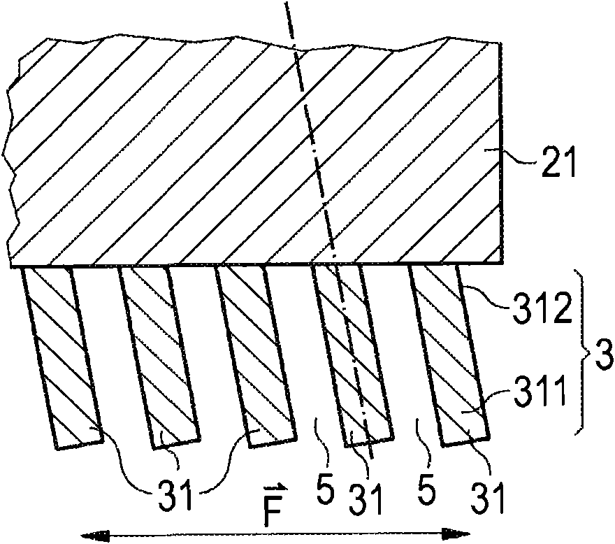
[0045] now refer to figure 1 , shows a vertical cross-sectional view of an assembly comprising an insulating substrate 2 soldered to a metal circuit substrate 1 , such as a metal plate or a heat sink, by means of an anchoring structure 3 . To this end, the metal substrate 1 may include a metal surface 1t configured to be flat or concave. When constructing the circuit substrate as a metal base plate for power semiconductor modules, even a slight protruding bend of the base plate is used to apply the injected thermal compound to spread the contact pressure more evenly over the heat sink, thereby minimizing the thermal Heat transfer resistance when the sink is mounted on the base plate. Instead of a pure metal substrate 1 any other type of circuit substrate can be used which is soldered on at least one side to the insulating substrate 2 when it comprises a solderable surface metallization. Where the circuit substrate is configured as a heat sink, it may have cooling fins and / or...
PUM
 Abstract
Description
Claims
Application Information
 - R&D Engineer
- R&D Manager
- IP Professional
- Industry Leading Data Capabilities
- Powerful AI technology
- Patent DNA Extraction
Browse by: Latest US Patents, China's latest patents, Technical Efficacy Thesaurus, Application Domain, Technology Topic, Popular Technical Reports.
© 2024 PatSnap. All rights reserved.Legal|Privacy policy|Modern Slavery Act Transparency Statement|Sitemap|About US| Contact US: help@patsnap.com


