Method for forming through hole at bottom of groove

A technology of grooves and substrates, which is applied in the manufacture of electrical components, semiconductor/solid-state devices, circuits, etc., can solve the problems of inability to form qualified patterned photoresist layer through holes, insufficient exposure, and inability to be reliably removed.

Inactive Publication Date: 2011-03-30
SEMICON MFG INT (SHANGHAI) CORP +1
View PDF2 Cites 8 Cited by
  • Summary
  • Abstract
  • Description
  • Claims
  • Application Information

AI Technical Summary

Problems solved by technology

[0014] The disadvantage of the prior art is that since the photoresist layer in the trench (that is, above the pre-formed via hole) is relatively thick, it is easy to cause insufficient exposure during the exposure process.
If the photoresist is not exposed enough, it cannot be removed during the development process, so a qualified patterned photoresist layer and subsequent via holes cannot be formed.

Method used


Image

  • Method for forming through hole at bottom of groove
  • Method for forming through hole at bottom of groove
  • Method for forming through hole at bottom of groove

Examples


Embodiment Construction

[0025] The specific implementation of the method for forming a through hole at the bottom of the trench provided by the present invention will be described in detail below with reference to the accompanying drawings.

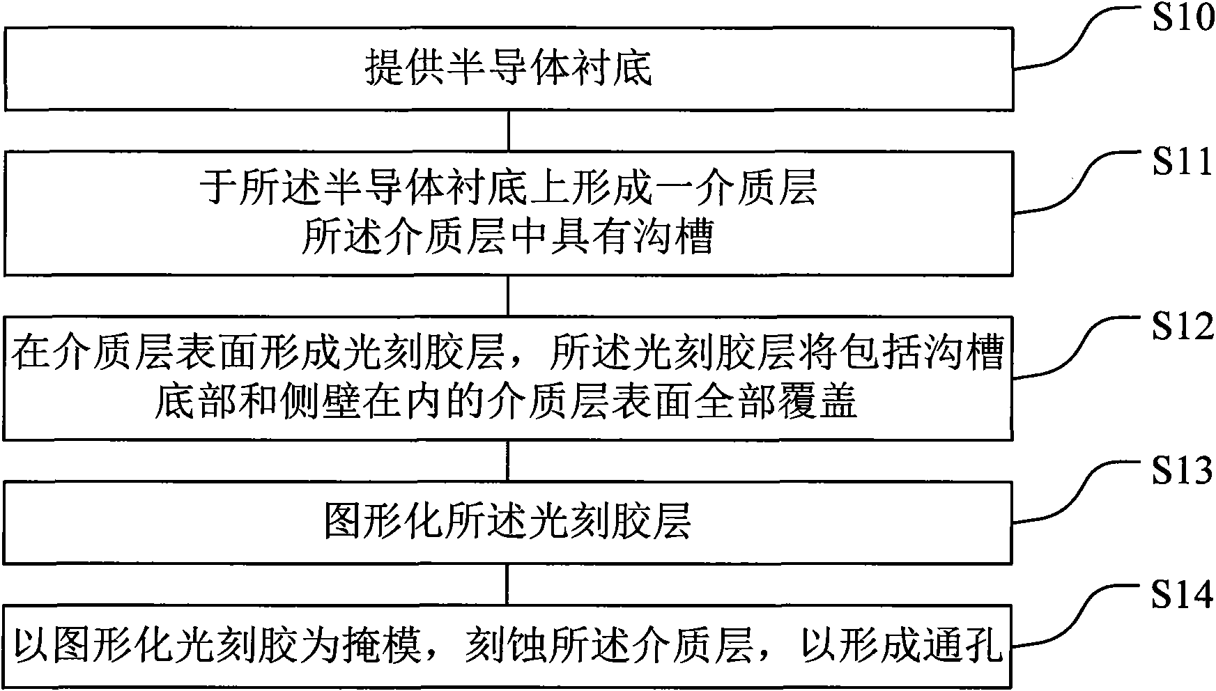
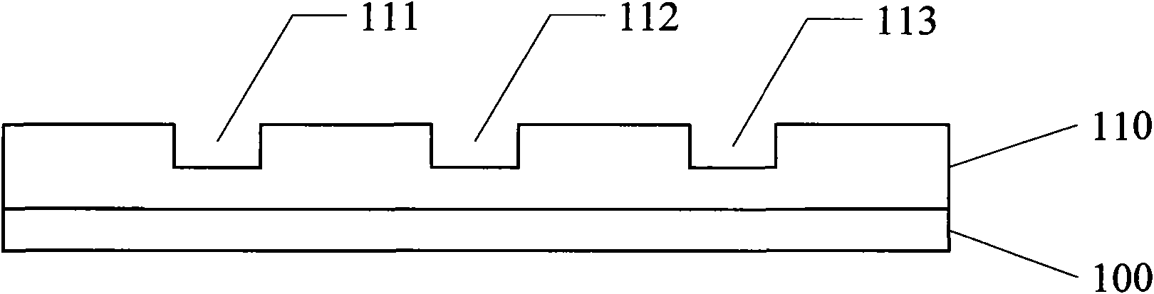
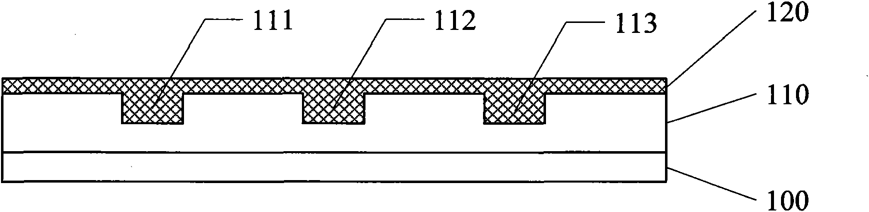
[0026] Attached Image 6 Shown is a flow chart of the implementation steps of this specific embodiment, including the following steps: step S20, providing a semiconductor substrate; step S21, forming a dielectric layer on the semiconductor substrate, the dielectric layer having trenches; S22, forming an anti-reflection layer on the surface of the dielectric layer, the anti-reflection layer covering the bottom and sidewalls of the trench; step S23, forming a photoresist layer on the surface of the anti-reflection layer; step S24, patterning the photoresist layer Step S25, using the patterned photoresist layer as a mask to etch the anti-reflection layer and the dielectric layer.

[0027] Attached Figure 7 Attached Picture 11 Shown is a schematic diagram of the proces...


PUM

PropertyMeasurementUnit
thicknessaaaaaaaaaa

Abstract

The invention relates to a method for forming a through hole at the bottom of a groove, comprising the following steps of: providing a semiconductor substrate; forming a dielectric layer on the semiconductor substrate, wherein the groove is arranged in the dielectric layer; forming an anti-reflecting layer on the surface of the dielectric layer, wherein the anti-reflecting layer covers the bottom and the side wall of the groove; forming a photoetching glue layer on the surface of the anti-reflecting layer; imaging the photoetching glue layer; and etching the anti-reflecting layer and the dielectric layer by using the imaged photoetching glue layer as a mask. The method has the advantages that before the photoetching glue layer is formed, one anti-reflecting layer is formed at the bottom of the groove so that the reflection of light on the surface of the groove is reduced, then photoetching glue can absorb more energy, and the method ensures that the photoetching glue in the groove can be fully exposed so as to ensure that the through hole is formed at the bottom of the groove in an etching process.

Description

【Technical Field】 [0001] The invention relates to the field of integrated circuit manufacturing, in particular to a method for forming a through hole at the bottom of a trench. 【Background technique】 [0002] The formation of trenches and vias on the surface of the intermetallic dielectric is a common process in the semiconductor process. The function of forming the trench is to be used to fill metal to form a metal wiring structure, and the function of the through hole at the bottom of the trench is to fill the metal to realize the electrical connection between the upper and lower layers of metal wiring. [0003] In the prior art, the usual manufacturing sequence is to first form a trench, and then form a through hole at the bottom of the trench. Attached figure 1 Shown is a flow chart of implementation steps of a method for forming a through hole at the bottom of a trench in the prior art, including the following steps: step S10, providing a semiconductor substrate, step S11, fo...

Claims


Application Information

Patent Timeline
Patent Type & Authority Applications(China)
IPC IPC(8): H01L21/768
Inventor 王新鹏黄怡尹晓明沈满华
Owner SEMICON MFG INT (SHANGHAI) CORP
Why Eureka
Try Eureka