Method for forming semiconductor device

A semiconductor and device technology, applied in the field of semiconductor device formation, can solve problems such as low efficiency, long production time, and inability to remove photoresist, and achieve the effect of improving etching efficiency and saving time

Active Publication Date: 2012-12-12
SEMICON MFG INT (SHANGHAI) CORP
View PDF0 Cites 0 Cited by
  • Summary
  • Abstract
  • Description
  • Claims
  • Application Information

AI Technical Summary

Problems solved by technology

[0005] The problem solved by the present invention is to provide a method for forming a semiconductor device, which prevents the problem that the photoresist residue cannot be removed due to long production time and low efficiency.

Method used


Image

  • Method for forming semiconductor device
  • Method for forming semiconductor device
  • Method for forming semiconductor device

Examples


Embodiment Construction

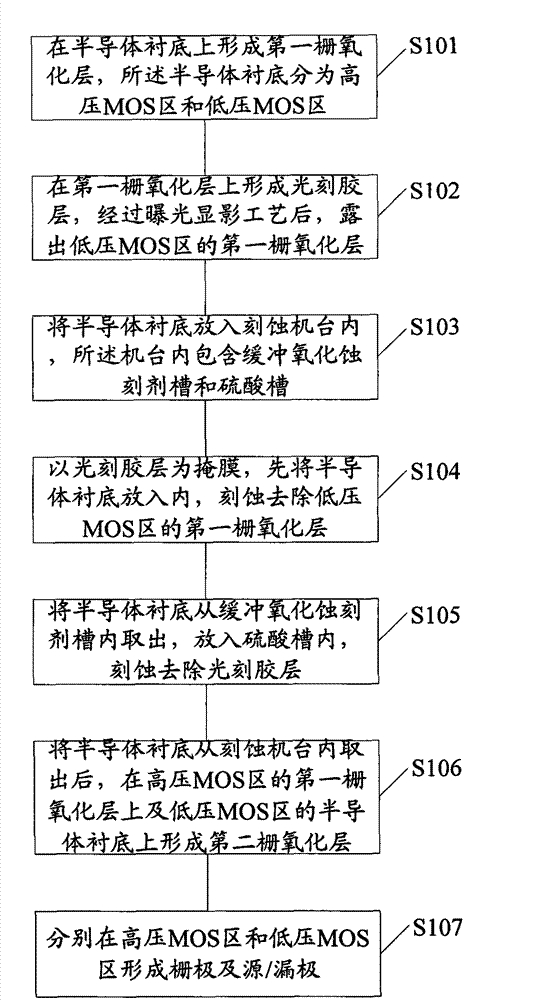
[0016] The essence of the present invention is to put the semiconductor substrate into the etching machine, which contains a buffered oxidation etchant tank and a sulfuric acid tank; after the first gate oxide layer is etched, it is not necessary to remove the semiconductor substrate from the The photoresist layer can be removed only by transferring the semiconductor substrate from the buffered oxidation etchant tank to the sulfuric acid tank in the same machine. The problem that photoresist residues cannot be removed due to too long waiting time between cleaning with buffered oxide etchant and cleaning with sulfuric acid is solved, time is saved, and etching efficiency is improved.

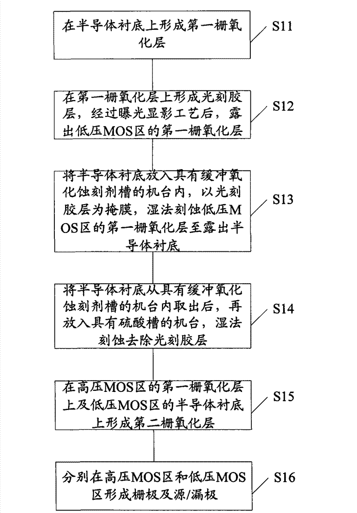
[0017] The process flow of the present invention to form a semiconductor device including a high-voltage MOS transistor and a low-voltage MOS transistor is as follows figure 2 As shown: step S101 is executed to form a first gate oxide layer on the semiconductor substrate, and the semiconductor s...


PUM

PropertyMeasurementUnit
thicknessaaaaaaaaaa
thicknessaaaaaaaaaa

Abstract

A method for forming a semiconductor device comprises the following steps: forming a first gate oxidation layer on a semiconductor substrate; forming a photoresist layer on the first gate oxidation layer and exposing the first gate oxidation layer of a low-pressure MOS area after exposure and development processes; placing the semiconductor substrate into an etching machine; taking the photoresist layer as the mask, firstly placing the semiconductor substrate into the photoresist layer and etching and removing the first gate oxidation layer of the low-pressure MOS area; taking the semiconductor substrate out of a buffering, oxidizing and etching agent groove, placing the semiconductor substrate into a sulfuric acid groove and etching and removing the photoresist layer; and after taking the semiconductor substrate out of the etching machine, forming second gate oxidation layers on the first gate oxidation layer of a high-pressure MOS area and the semiconductor substrate of the low-pressure MOS area, wherein the semiconductor substrate is divided into the high-pressure MOS area and the low-pressure MOS area; and the machine comprises the buffering, oxidizing and etching agent grooveand the sulfuric acid groove. The method saves time, improves the etching efficiency and can solve the problem that the photoresist residue can not be removed.

Description

technical field [0001] The present invention relates to a method of forming a semiconductor device. Background technique [0002] In semiconductor technology, even though the device size continues to shrink, it is still desirable to improve the performance of transistors, and it is also desirable to manufacture integrated circuit semiconductor devices that combine low, high, and medium voltage applications. For example, integrated circuits (hereinafter referred to as driver ICs) used to drive image sensors, LCDs, and printed magnetic heads, etc., are composed of ICs with strong withstand voltage between the drain and source that operate at a power supply voltage above +V. The drive output unit of the high-voltage MOS transistor and the logic unit of the control drive output unit of the low-voltage MOS transistor that can be used at a power supply voltage of several volts or less have poor drain withstand voltage capability. Such integrated circuits are often referred to as ...

Claims


Application Information

Patent Timeline
Patent Type & Authority Patents(China)
IPC IPC(8): H01L21/8234H01L21/311G03F7/42
Inventor 杜学东韦磊陈美丽
Owner SEMICON MFG INT (SHANGHAI) CORP
Why Eureka
Try Eureka