Compensating device for synchronous rectification control and method thereof

A technology of synchronous rectification and compensation method, which is applied in the direction of output power conversion device, AC power input conversion to DC power output, electrical components, etc.

Active Publication Date: 2011-03-30
DELTA ELECTRONICS INC
View PDF4 Cites 11 Cited by
  • Summary
  • Abstract
  • Description
  • Claims
  • Application Information

AI Technical Summary

Problems solved by technology

Therefore, there is indeed a significant gap between the two situ

Method used


Image

  • Compensating device for synchronous rectification control and method thereof
  • Compensating device for synchronous rectification control and method thereof
  • Compensating device for synchronous rectification control and method thereof

Examples


Embodiment Construction

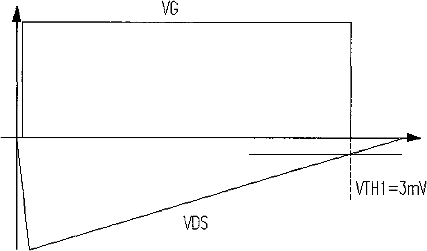
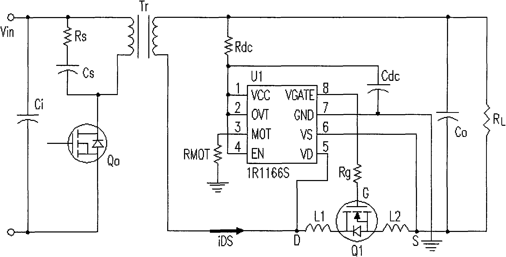
[0047] see Figure 7 , which is the first equivalent circuit diagram of a basic principle of the present invention, which is a comparator. Before VDS (=VD-VS) is compared with a threshold value VTH, a and iDS (ie- iSD) related compensation voltage Vcomp to reduce or eliminate the influence of parasitic inductance.

[0048] see again Figure 8 , which is the second equivalent circuit diagram of a basic principle of the present invention, which is also a comparator. Before VDS (=VD-VS) is compared with a threshold value VTH, a value related to iDS is added to the VD end first. Compensation voltage Vcomp to reduce or eliminate the influence of parasitic inductance.

[0049] in Figure 7 and Figure 8 The magnitude of Vcomp and whether it is positive or negative (ie, Vcomp is greater than zero or less than zero) depends on the desired reduction or elimination of the effects of parasitic inductance.

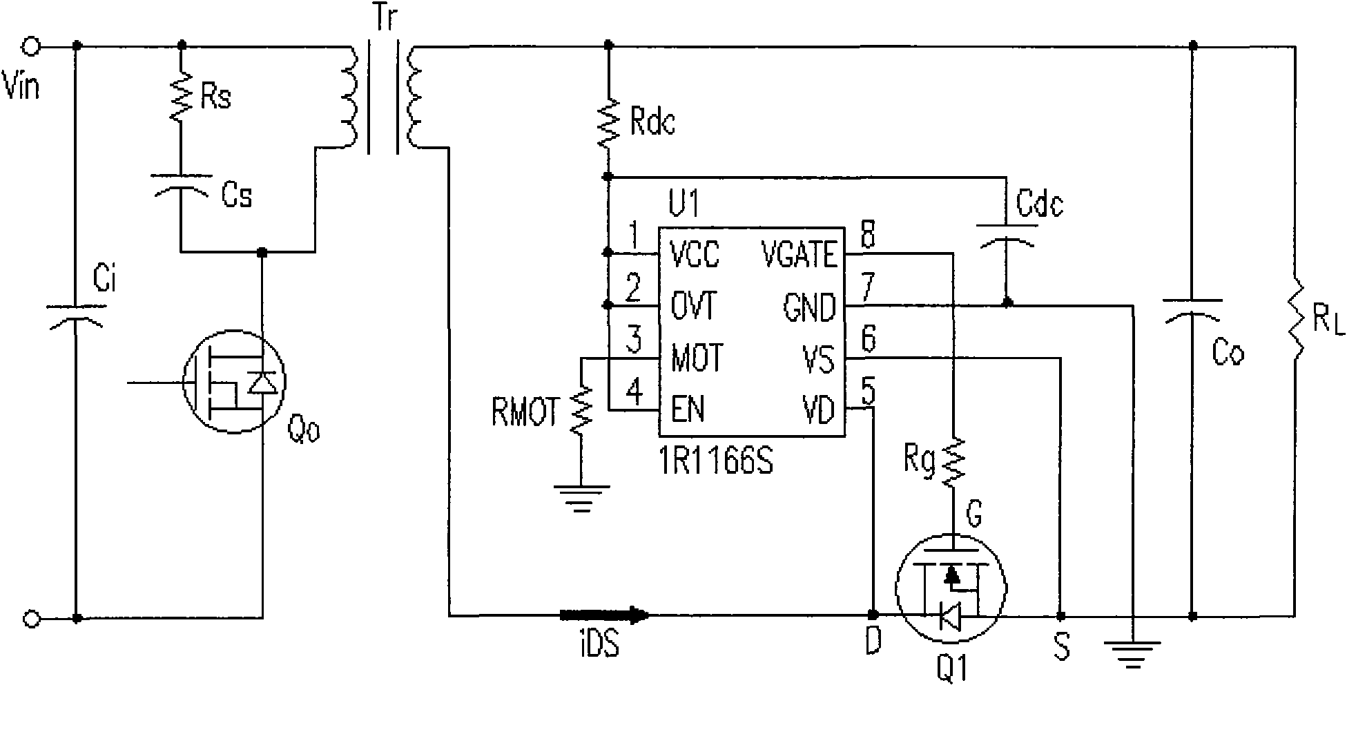
[0050] exist Figure 9 , which shows a circuit diagram of a prior art reson...


PUM


Abstract

The invention discloses a compensating device arranged at a circuit comprising a synchronous rectification switch, a controller and a load, and a method thereof, wherein the synchronous rectification switch comprises a first end, a first inductor, a second end and a second inductor, wherein the first inductor is electrically connected in series with the first end, the second inductor is electrically connected in series with the second end, the controller is coupled with the first inductor and the second inductor, in addition, the device comprises a voltage source, and the voltage source comprises a positive electrode end and a negative electrode end, wherein the positive electrode end is coupled with the controller, and the negative electrode is coupled with the second inductor; and the compensating device is used for providing a compensating voltage so as to eliminate or reduce the influence on a voltage value between the first end and the second end caused by the first inductor and the second inductor.

Description

technical field [0001] The invention relates to a compensation device for synchronous rectification switches, in particular to a voltage compensation device for synchronous rectification switches. Background technique [0002] Synchronous rectifier circuits can be used to improve the efficiency of switching power supplies, especially in applications with low voltage and high output current. Therefore, the application of synchronous rectifier circuits is becoming more and more extensive, and the improvement of its shortcomings is also paid more and more attention. E.g, figure 1 Shown is a schematic circuit diagram of a flyback converter with a synchronous rectifier switch and no parasitic inductance in the prior art. The flyback converter receives an input voltage Vin, and includes an input capacitor Ci, a conversion circuit stage, a transformer Tr, a synchronous rectifier circuit, an output circuit stage and a load RL. The conversion circuit stage includes a resistor Rs, ...

Claims


Application Information

Patent Timeline
IPC IPC(8): H02M7/217
Inventor 楼俊山焦德智林栋
Owner DELTA ELECTRONICS INC
Why Eureka
Try Eureka