High-power semiconductor laser array fast and slow axis beam quality homogenization device

A laser array and semiconductor technology, applied in the field of laser technology applications, can solve the problems of poor control of precise positioning between prisms and difficult assembly

Inactive Publication Date: 2011-04-06
BEIJING UNIV OF TECH
View PDF6 Cites 10 Cited by
  • Summary
  • Abstract
  • Description
  • Claims
  • Application Information

AI Technical Summary

Problems solved by technology

The disadvantage of this method is that the precise positioning between the prisms is not easy to control, and the assembly is difficult

Method used


Image

  • High-power semiconductor laser array fast and slow axis beam quality homogenization device
  • High-power semiconductor laser array fast and slow axis beam quality homogenization device
  • High-power semiconductor laser array fast and slow axis beam quality homogenization device

Examples


Embodiment approach

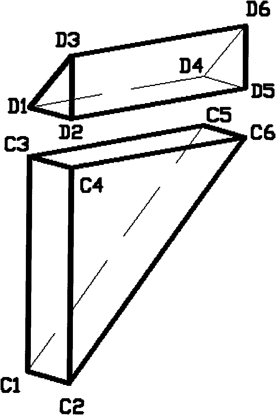
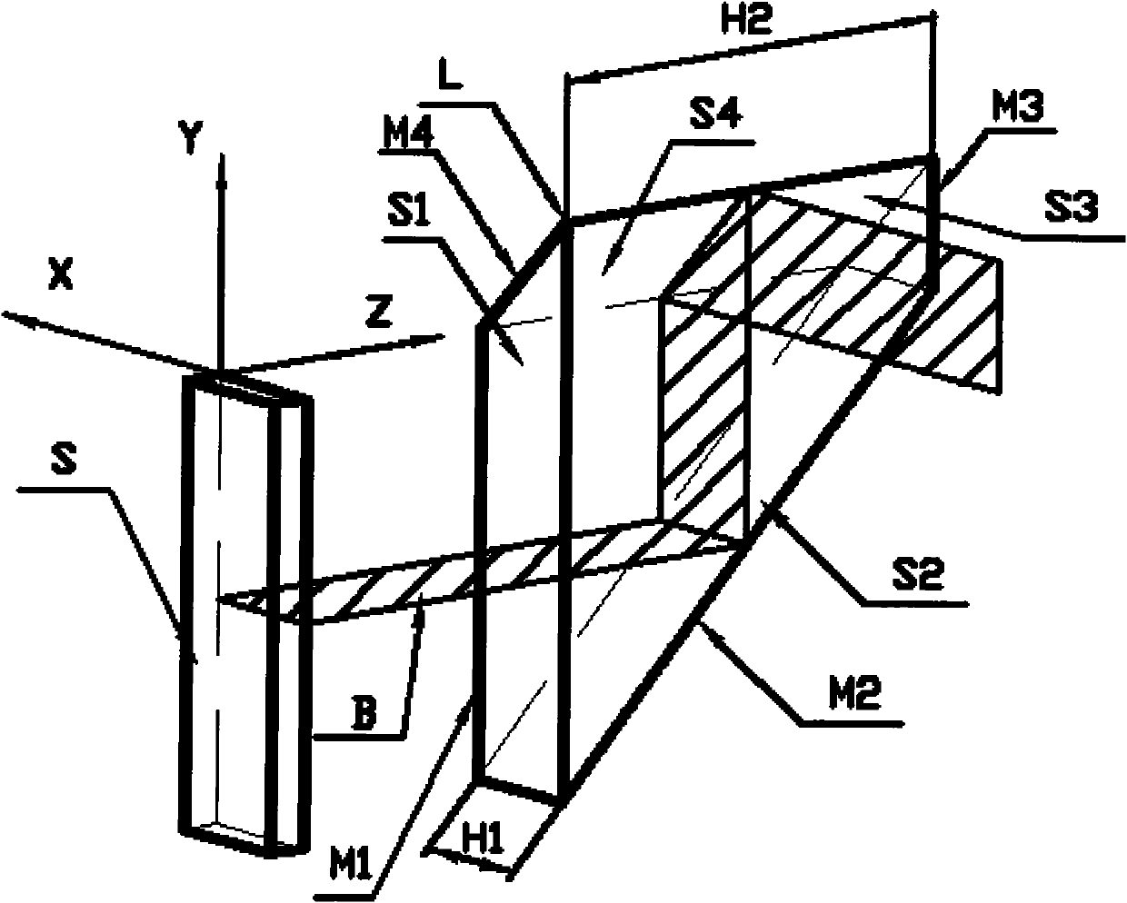
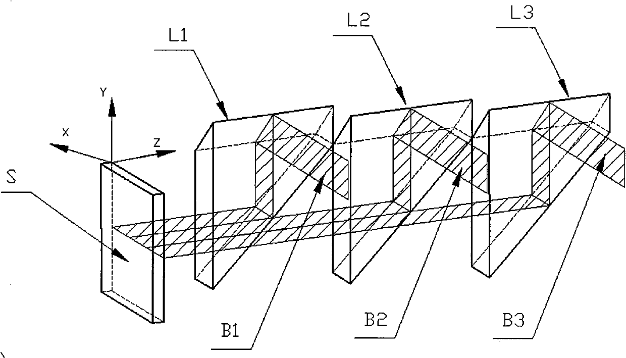
[0026] In this embodiment, the semiconductor laser beam is divided into three parts in the direction of the slow axis, and the structure of the shaping device is as follows: image 3As shown, it includes a semiconductor laser array S, an improved first isosceles right-angle prism L1, an improved second isosceles right-angle prism L2, and an improved third isosceles right-angle prism L3 placed in sequence along the light propagation direction. The structures of the improved isosceles right-angle prisms L1, L2 and L3 are exactly the same, but the placement positions are different. All the prisms are placed in parallel along the direction of the slow axis of the semiconductor laser array, staggered forward and backward by a certain distance, and distributed in a ladder shape. The first surface S1 of all prisms staggered forward and backward by a certain distance, that is, surface C1C2C4C3, performs beam cutting on the slow axis of the laser array, and passes through the second su...


PUM


Abstract

The invention relates to a high-power semiconductor laser array shaping device, and belongs to the field of application of laser technology. The device comprises a group of improved isosceles right-angle prisms, wherein the improved isosceles right-angle prisms in the prism group have identical size and structure and are arranged at different positions; all prisms are parallelly arranged along the direction of a slow axis of a semiconductor laser array in a ladder-like distribution mode and staggered at certain intervals front and back; the slow axis of the laser array is subjected to beam cutting by first surfaces of all the prisms staggered at certain intervals front and back, and beams pass through second surfaces which form an angle of 45degrees with the first surfaces to be subjected to total reflection; and the beams subjected to total reflection meet third surfaces which form an angle of 45 degrees with both the first surfaces and the second surfaces to be subjected to total reflection again, so that the effect of cutting and rearranging the beams is achieved. The device has high efficiency, is particularly suitable for high-power semiconductor laser beam shaping, has the advantages of low cost and the like, and is convenient to install and adjust.

Description

technical field [0001] The invention relates to beam shaping of a semiconductor laser array, which is a device for homogenizing the product of fast and slow axis optical parameters of the semiconductor laser array, and belongs to the application field of laser technology. Background technique [0002] Semiconductor lasers have the advantages of high electro-optical conversion efficiency, small size, light weight, etc., making their applications more and more extensive. However, compared with other lasers, the beam quality of semiconductor lasers is relatively poor, the beam divergence angle is large, and the far-field light intensity has an elliptical Gaussian distribution, which makes it difficult to focus, which limits its further development to a certain extent. In order to meet the requirements of the application, the beam of the semiconductor laser must be shaped first. The research on semiconductor lasers is developing towards the direction of high power and high beam...

Claims


Application Information

Patent Timeline
Patent Type & Authority Applications(China)
IPC IPC(8): G02B27/09
Inventor 王智勇刘友强曹银花
Owner BEIJING UNIV OF TECH
Why Eureka
Try Eureka