Measuring structure for improving accuracy of exposure conditions

A technology of exposure conditions and accuracy, applied in the field of measuring structures, can solve problems such as reducing production capacity, and achieve the effect of improving height difference, good flatness, and improving accuracy

Inactive Publication Date: 2011-04-06
CSMC TECH FAB1
View PDF0 Cites 2 Cited by
  • Summary
  • Abstract
  • Description
  • Claims
  • Application Information

AI Technical Summary

Problems solved by technology

However, increasing the measurement points will inevitably increase the area for testing on the wafer surface. For highly integrated chips and related devices, the production capacity will be greatly reduced. For the production of chips and devices, especially highly integrated The production of high-speed chips and devices has a greater impact

Method used


Image

  • Measuring structure for improving accuracy of exposure conditions
  • Measuring structure for improving accuracy of exposure conditions
  • Measuring structure for improving accuracy of exposure conditions

Examples


Embodiment Construction

[0013] In order to make the object, technical solution and advantages of the present invention clearer, the present invention will be further described in detail below in conjunction with the accompanying drawings.

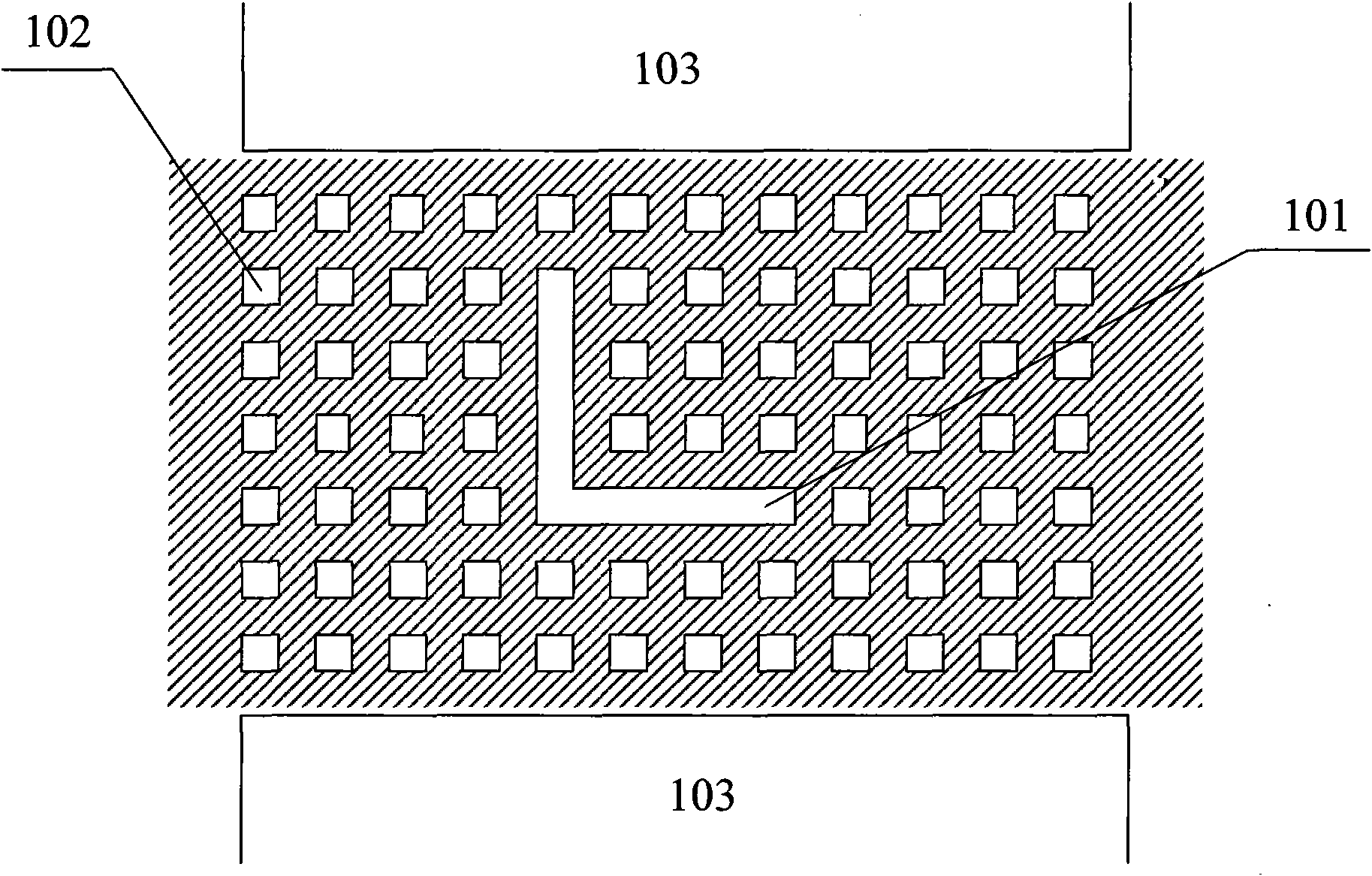
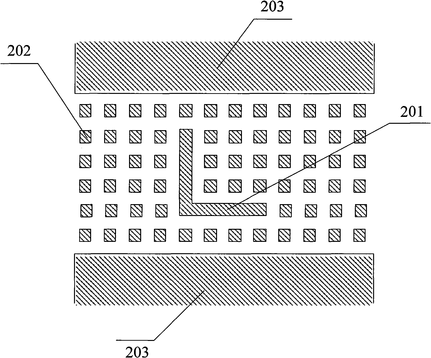
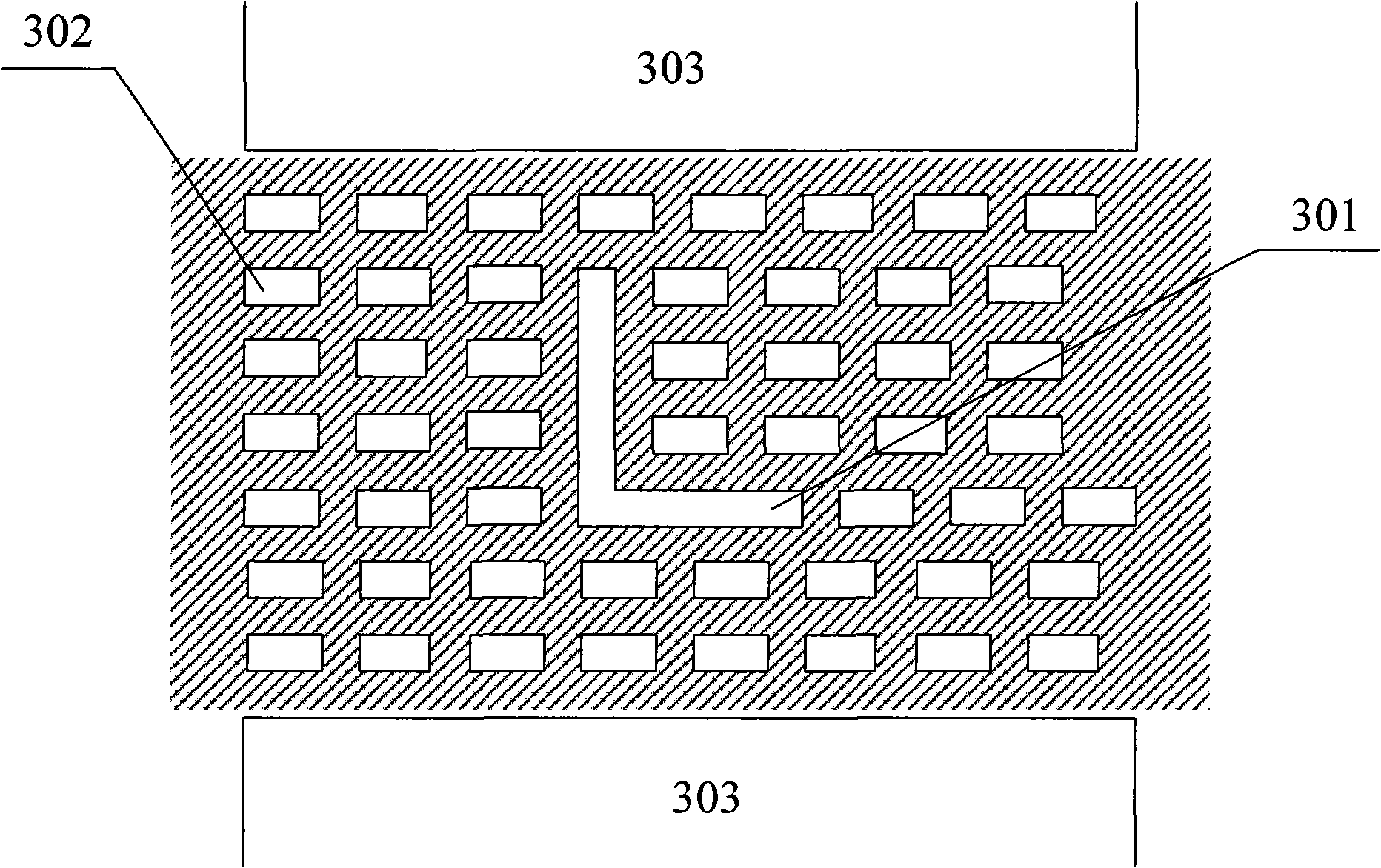
[0014] figure 1 It is a structural schematic diagram of the first embodiment of the measurement structure for improving the accuracy of exposure conditions provided by the present invention.

[0015] Such as figure 1 As shown, the measurement structure for improving the accuracy of exposure conditions includes a main pattern 101 and a dummy pattern 102 . Among them, the main pattern 101 is a measurement pattern located on the dicing line for determining the exposure conditions of lithography, and its characteristic size is basically consistent with the characteristic size of the pattern of the internal device area 103 of the chip, which can correctly reflect the shape and shape of the pattern of the internal device area 103 of the chip. size features, but the pa...


PUM


Abstract

The invention provides a measuring structure for improving the accuracy of exposure conditions, belonging to the technical field of semiconductors. The measuring structure comprises a main graph and a dummy graph, wherein the dummy graph is located beside the main graph; the density of the whole graph of the measuring structure is similar to the density of the graph in a device area inside the chip so that the measuring graph and the graph of the device area inside the chip are ensured to have approximately identical grinding velocity in the chemical and mechanical polishing process and the whole wafer is ensured to be more flattened. During photoetching exposure, the measuring graph and the optimum imaging focus in the device area inside the chip are located on the same plane, and the exposure condition defined by measuring the measuring graph is the optimum exposure condition of the graph of the device area inside the chip, thereby the accuracy of the photoetching exposure condition is effectively improved without affecting the capacity.

Description

technical field [0001] The invention relates to semiconductor photolithography exposure technology, in particular to a measurement structure for determining exposure conditions, and belongs to the field of semiconductor technology. Background technique [0002] In the manufacturing process of semiconductor chips and devices, a measurement structure including measurement patterns is usually arranged in the dicing line on the surface of the wafer to determine the photolithographic exposure conditions of the entire wafer. In the prior art, when performing photolithography, the optimum exposure conditions of the entire wafer can be defined and the process window can be judged by measuring only the measurement pattern located in the dicing line. In the prior art, the method of defining the exposure conditions of the entire wafer by only measuring the measurement pattern located in the dicing line has very high requirements for the flatness of the wafer surface. Only when the wafe...

Claims


Application Information

Patent Timeline
Patent Type & Authority Applications(China)
IPC IPC(8): G03F7/20
Inventor 胡俊张辰明杨耀华刘志成
Owner CSMC TECH FAB1
Why Eureka
Try Eureka