Semiconductor device structures and related processes

A device structure, semiconductor technology, applied in the direction of semiconductor devices, semiconductor/solid-state device manufacturing, electrical components, etc.

Active Publication Date: 2011-04-06
MAXPOWER SEMICON INC
View PDF4 Cites 33 Cited by
  • Summary
  • Abstract
  • Description
  • Claims
  • Application Information

AI Technical Summary

Problems solved by technology

[0005] As switching speed requirements for new applications increase to 1MHz and beyond, state

Method used


Image

  • Semiconductor device structures and related processes
  • Semiconductor device structures and related processes
  • Semiconductor device structures and related processes

Examples


Embodiment Construction

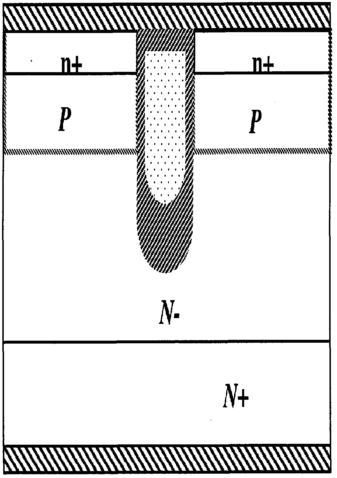
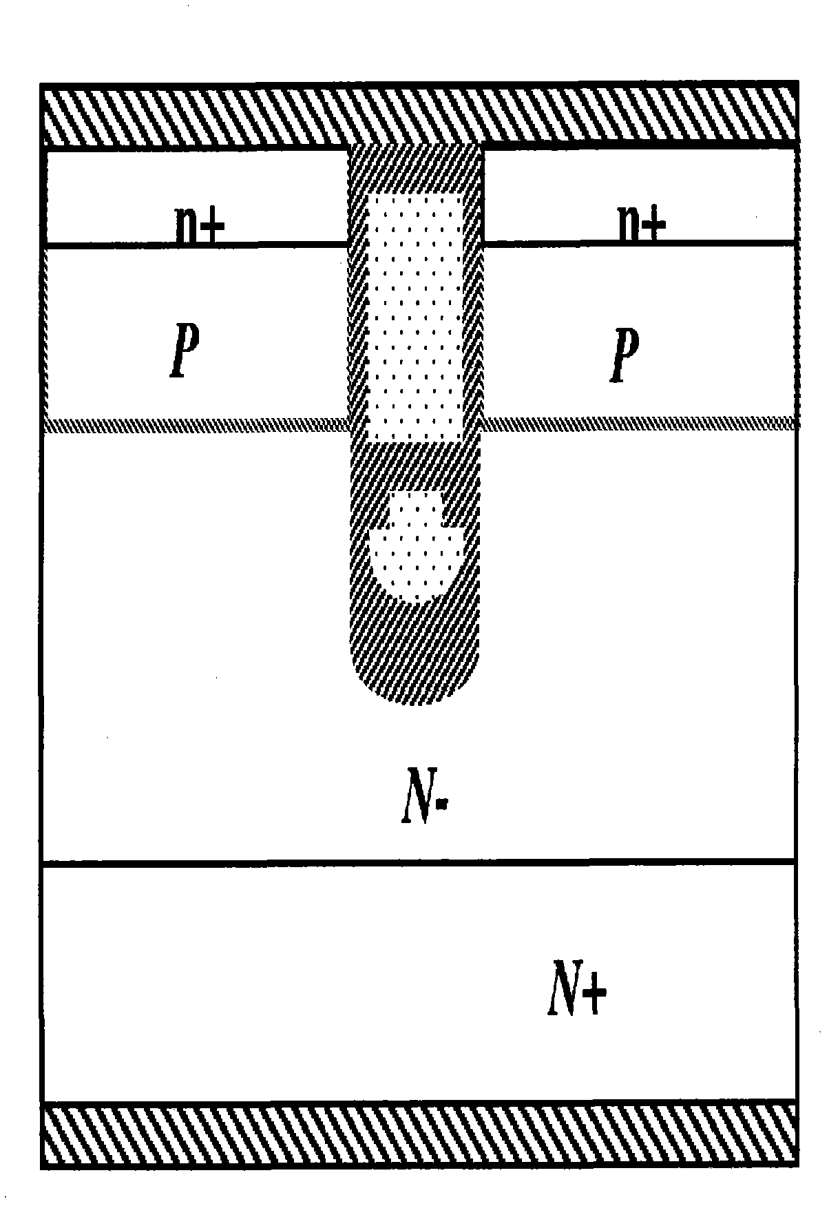
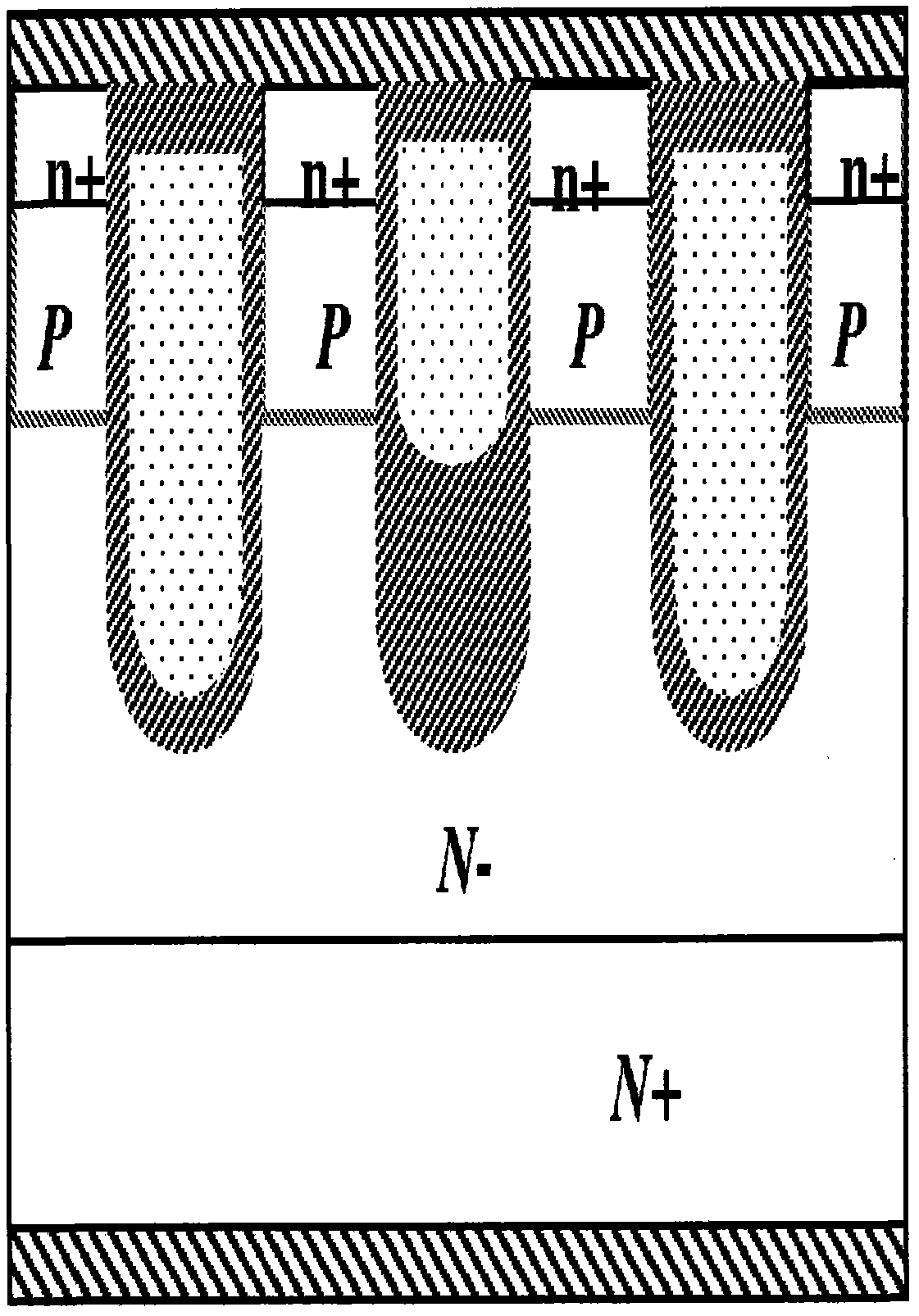
[0032] The many innovative solutions of the present application will be described herein with particular reference to the presently preferred embodiments (as examples, not limitations). This application describes several embodiments, but the following statements should not generally be taken as limitations on the claims.

[0033] For simplicity and clarity of illustration, the drawings illustrate the general manner of construction, and descriptions and details of well-known features and techniques are omitted to avoid unnecessarily obscuring the present invention. In addition, components in the drawings are not necessarily drawn to scale, and certain areas or components may be enlarged to facilitate a further understanding of the embodiments of the present invention.

[0034] Words such as "first", "second", "third", "fourth" (if any) in the description and claims may be used to identify similar components and need not be used to describe a specific order or chronological ord...


PUM


Abstract

Improved highly reliable power RFP structures and fabrication and operation processes. The structure includes plurality of localized dopant concentrated zones beneath the trenches of RFPs, either floating or extending and merging with the body layer of the MOSFET or connecting with the source layer through a region of vertical doped region. This local dopant zone decreases the minority carrier injection efficiency of the body diode of the device and alters the electric field distribution during the body diode reverse recovery.

Description

[0001] Cross-references to related applications [0002] This application claims priority to US Provisional Application Serial No. 61 / 065,759, filed February 14, 2008, which is hereby incorporated by reference in its entirety. technical field [0003] The invention relates to a field effect transistor and a method, in particular to a highly reliable power insulated gate field effect transistor (MOSFET) with a recessed field plate (RFP, Recessed Field Plate) and related technologies. Background technique [0004] Power MOSFETs are widely used as switching devices in many electronic applications. In order to minimize conduction power loss, the MOSFET must have a low specific on-resistance, which is defined as the product of the on-resistance area (R on *A), where R on is the MOSFET resistance when the MOSFET is in the on state, and A is the area of ​​the MOSFET. Trench MOSFETs offer low specific on-resistance, especially in the 10-100 voltage range. As unit density increas...

Claims


Application Information

Patent Timeline
IPC IPC(8): H01L21/336H01L29/78
CPCH01L29/1095H01L29/7811H01L29/7813H01L29/0623H01L29/0878H01L21/26586H01L29/66734H01L29/0696H01L29/0634H01L29/42368H01L29/407H01L29/66727H01L29/41766H01L29/41
Inventor 曾军穆罕默德·恩·达维希
Owner MAXPOWER SEMICON INC
Why Eureka
Try Eureka