Metallizing manufacturing method of ceramic substrate

A technology for ceramic substrates and manufacturing methods, applied in the field of metallization of ceramic substrates, capable of solving problems such as easy formation of copper oxide, lower product quality, and increased manufacturing costs

Inactive Publication Date: 2011-04-13
HOLY STONE ENTERPRISE
View PDF3 Cites 6 Cited by
  • Summary
  • Abstract
  • Description
  • Claims
  • Application Information

AI Technical Summary

Problems solved by technology

However, the existing circuit layer used on the ceramic substrate is to tightly adhere the metal material layer to the ceramic substrate by means of thermocompression. It is necessary to use a thicker metal material layer to be attached to the ceramic substrate, and the joint surface is easy to Copper oxide (CuO) is formed, causing an increase in thermal resistance
If the metal material layer is too thin, it will cause cracks in the metal material layer during the thermocompression bonding process, resulting in lower product quality and increased manufacturing costs.

Method used


Image

  • Metallizing manufacturing method of ceramic substrate
  • Metallizing manufacturing method of ceramic substrate
  • Metallizing manufacturing method of ceramic substrate

Examples


Embodiment Construction

[0012] In order to achieve the above-mentioned purpose and structure, the technical means adopted by the present invention and their effects, the above-mentioned and other technical features and advantages of the present invention will be described in more detail below in conjunction with the accompanying drawings and preferred embodiments of the present invention.

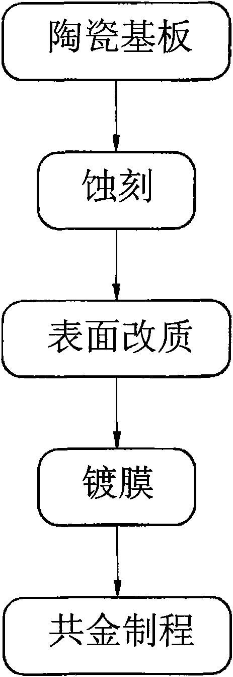
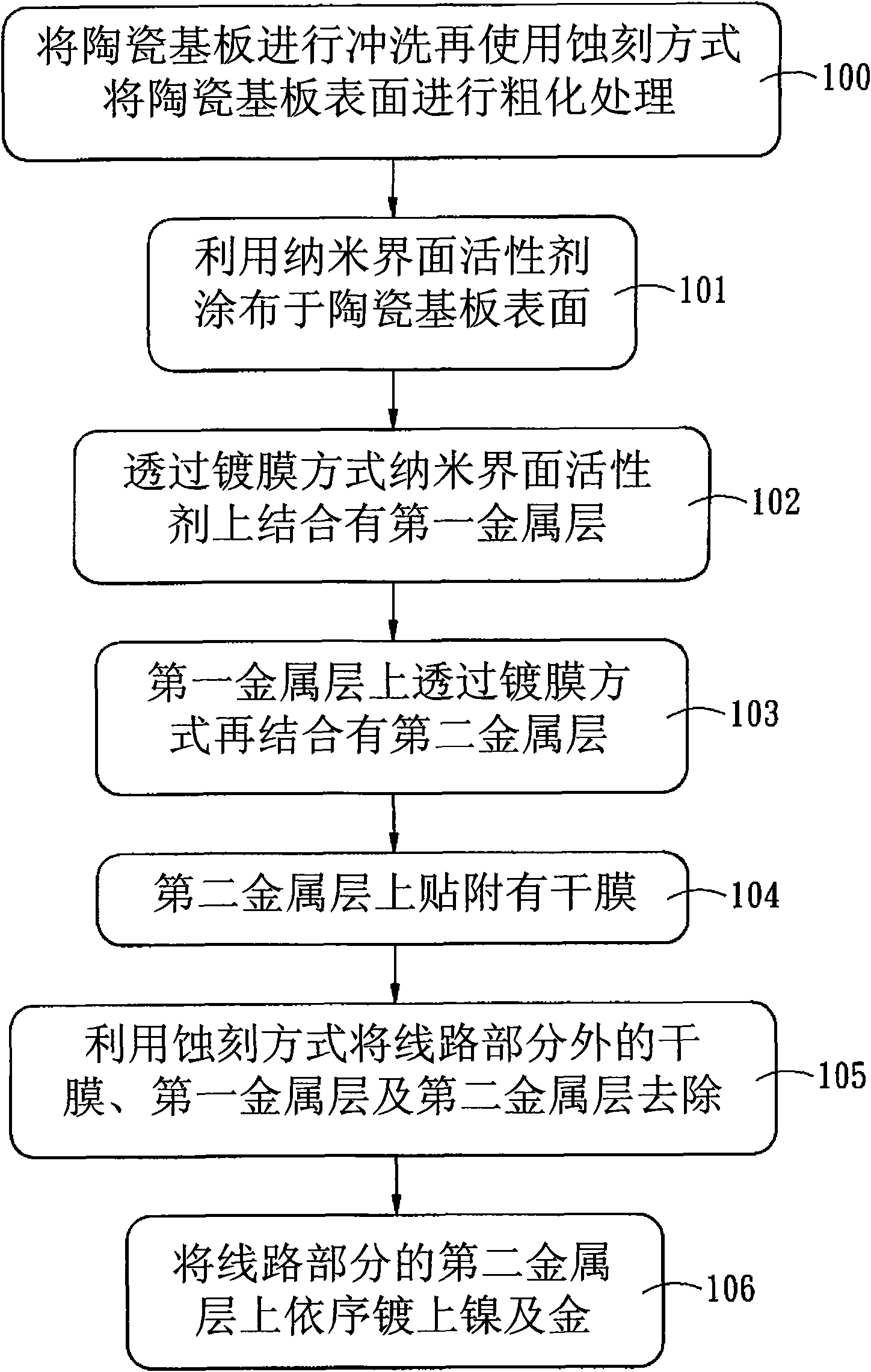
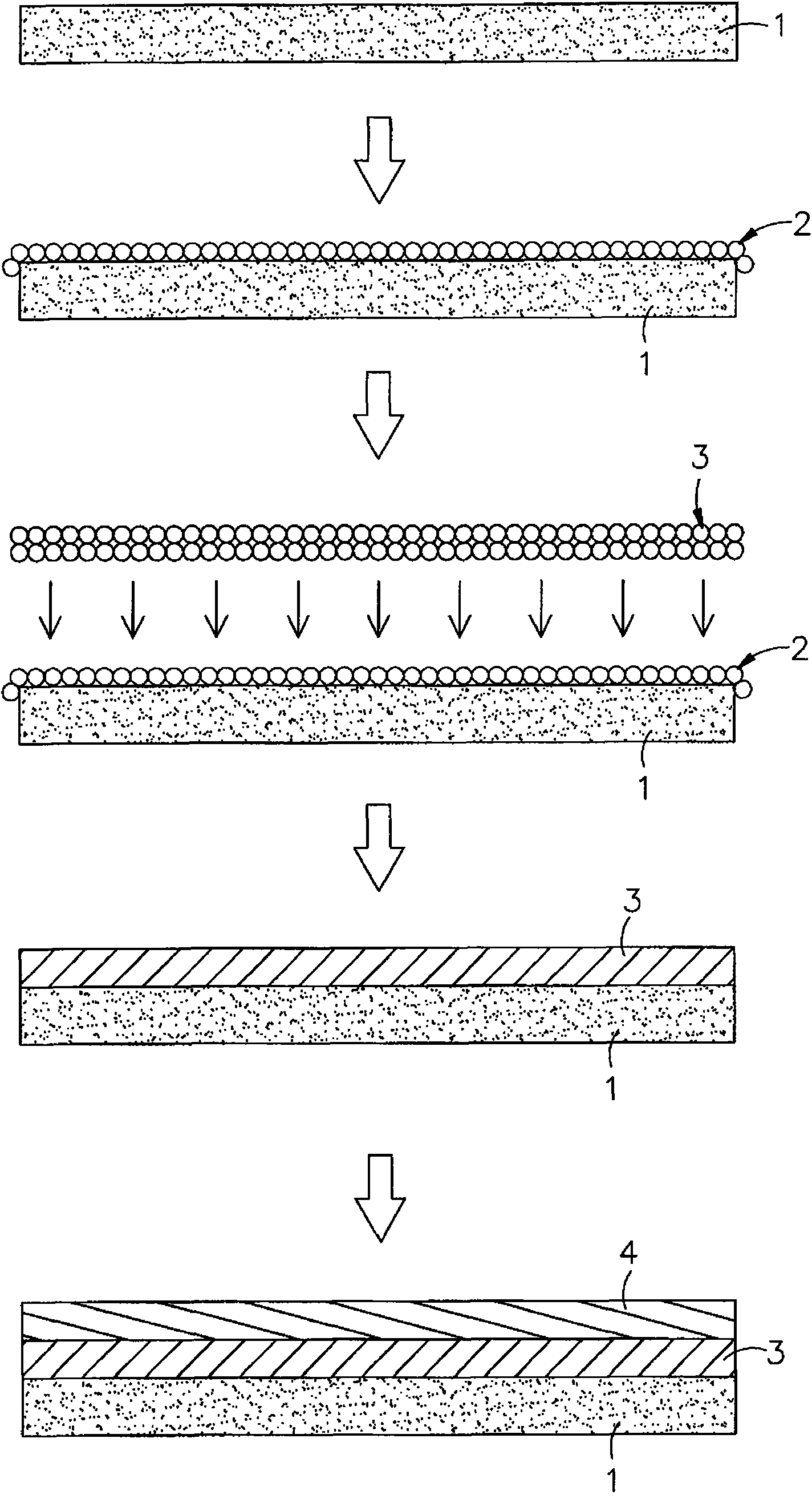
[0013] figure 1 , figure 2 , image 3 , Figure 4 As shown, they are respectively the architecture flow chart, step flow chart, production step diagram (1) and production step diagram (2) of the present invention. It can be clearly seen from the figure that the metallization manufacturing method of the ceramic substrate of the present invention can be manufactured by the following steps, the steps are:

[0014] (100) The ceramic substrate 1 is cleaned, and then the surface of the ceramic substrate 1 is roughened by micro-etching.

[0015] (101) Coating the surface of the ceramic substrate 1 with the nanosurfa...


PUM

PropertyMeasurementUnit
thicknessaaaaaaaaaa

Abstract

The invention provides a metallizing manufacturing method of a ceramic substrate, in particular to a film coating manufacturing way utilized because the ceramic substrate is an inorganic substance without any positive and negative electrical property and is very difficult to joint with metal. The film coating manufacturing way comprises the following steps of: firstly cleaning the ceramic substrate; carrying out roughening treatment on the surface of the ceramic substrate in a micro-etching way; and coating nanometer grade Si-containing surfactants on the surface of the ceramic substrate to enable the surface of the ceramic substrate, without electric polarity, to generate negative electrode effect. Therefore, a positively charged first metal layer which has thinner thickness and is easy to joint with ceramic can be deposited on the nanometer grade Si-containing surfactants in the film coating way, and the effect of effectively reducing the manufacturing cost of the ceramic substrate, which has fine heat positively charged, good electrical property, high reliability and strong bonding force, can be achieved.

Description

technical field [0001] The present invention provides a method for metallizing ceramic substrates, particularly involving the use of nano surfactants to coat the surface of roughened ceramic substrates, so that positive and negative electrode effects can be produced on the surface of ceramic substrates that do not have electrical polarity. In this way, The first metal layer with a relatively thin thickness can be deposited on the ceramic substrate with the nano-surfactant through electroplating thin film, so as to achieve the effect meeting the market demand. Background technique [0002] At present, with the rapid development of science and technology and the pursuit of higher quality of life, the application characteristics of many products tend to be extremely strict, making the use of newly developed materials a necessary means. Today's integrated circuit packaging is affected by the pursuit of better transmission efficiency and miniaturization (such as electronic compon...

Claims


Application Information

Patent Timeline
Patent Type & Authority Applications(China)
IPC IPC(8): C04B41/88C04B41/90C04B41/91
Inventor 林文新刘吉仁
Owner HOLY STONE ENTERPRISE
Why Eureka
Try Eureka