Forming method of through hole

A via-hole and patterning technology, applied in electrical components, semiconductor/solid-state device manufacturing, circuits, etc., to save process operation time, save costs, and reduce standing wave effects

Inactive Publication Date: 2011-04-20
SEMICON MFG INT (SHANGHAI) CORP
View PDF2 Cites 2 Cited by
  • Summary
  • Abstract
  • Description
  • Claims
  • Application Information

AI Technical Summary

Problems solved by technology

[0016] In order to solve the problem in the prior art, the standing wave effect will occur during the exposure process of the photoresist layer, so that the side of the photoresist layer formed after development has a wide burr structure, and the quality o

Method used


Image

  • Forming method of through hole
  • Forming method of through hole
  • Forming method of through hole

Examples


Embodiment 1

[0056] The method for forming the via hole in this embodiment includes:

[0057] Firstly, a substrate is provided, and a dielectric layer is provided on the substrate;

[0058] Secondly, coating a photoresist layer on the dielectric layer;

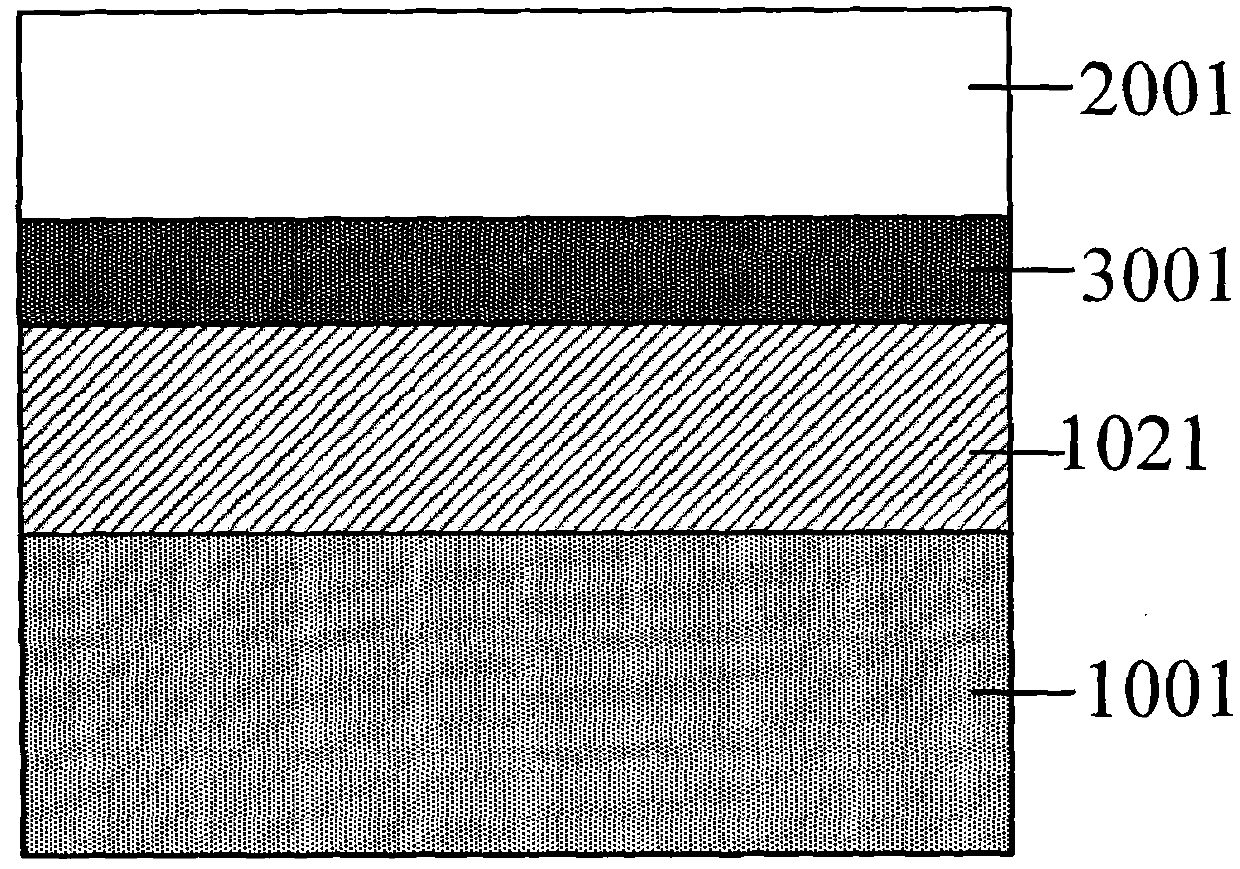
[0059] Figure 2A Shown is a schematic cross-sectional view of the substrate after coating the photoresist layer on the substrate, as Figure 2A As shown, there is a dielectric layer 102 on the substrate 100, and a photoresist layer 200 is coated on the dielectric layer 102;

[0060] Preferably, a dye is added into the photoresist layer, and the dye can reduce light interference;

[0061] Preferably, it also includes: performing post-baking (PEB, Post Exposure Baking) and hard-baking (HB, Hard Baking) on ​​the photoresist layer to reduce the standing wave effect;

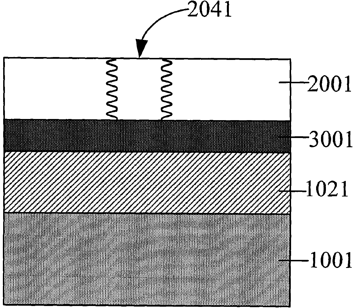
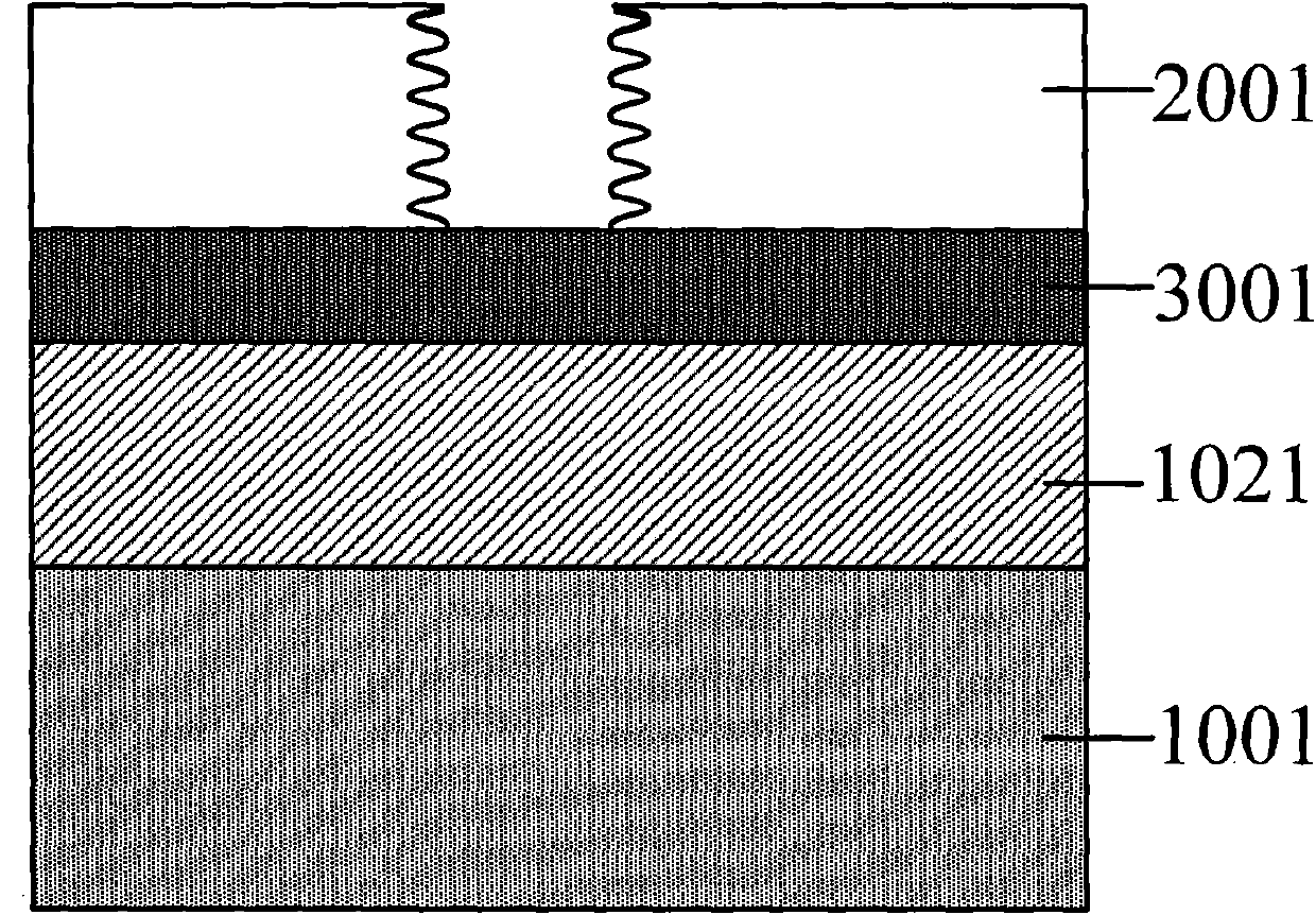
[0062] Secondly, patterning the photoresist layer by exposure;

[0063] Figure 2B It is a schematic cross-sectional view of the substrate after exposing the photoresist, su...

Embodiment 2

[0079] Figure 3F It is a flow chart of a method for forming a via hole in an embodiment, referring to Figure 3F As shown, the method for forming the via hole in this embodiment is described in detail, including:

[0080] Firstly, a substrate is provided, on which a dielectric layer and a bottom anti-reflection layer are sequentially arranged;

[0081] The bottom antireflective coating (BARC, Bottom Anti-Reflective Coating) is located at the bottom of the photoresist layer, and is used to reduce the reflection of light at the bottom of the photoresist layer; the material of the bottom antireflective layer can be an organic antireflective coating ( Organic), which is formed by spin coating, and the organic reflective coating can directly receive the incident light; the material of the bottom antireflective layer can also be an inorganic antireflective coating (Inorganic), which uses plasma enhanced chemical vapor phase Formed by deposition (PECVD, Plasma Enhanced Chemical Va...


PUM

PropertyMeasurementUnit
Thicknessaaaaaaaaaa
Thicknessaaaaaaaaaa

Abstract

The invention provides a forming method of a through hole, which comprises the steps of: providing a substrate, wherein a medium layer is arranged on the substrate; coating a photoresistance layer on the medium layer; imaging the photoresistance in an exposure manner; developing the photoresistance layer to remove the photoresistance layer of the exposure layer; oxidizing the photoresistance layer; and etching the medium layer by using left photoresistance layer to form a through hole, and removing the left photoresistance layer. The forming method of the through hole solves the problem of wider burr structure generated by standing wave effect during the exposure of the photoresistance layer, ensures that the quality of the formed through hole is better, and is beneficial to the reduction of the production cost.

Description

technical field [0001] The invention relates to the technical field of semiconductor manufacturing, in particular to a method for forming via holes in the production of semiconductor devices. Background technique [0002] With the continuous miniaturization of semiconductor devices, the requirements for the precision and fineness of semiconductor processes are getting higher and higher, especially the production of vias connecting different conductive layers of semiconductor devices is becoming more and more difficult, because vias The size of the via hole is much smaller than that of the semiconductor device, however, the quality of the via hole directly affects whether the semiconductor device can work. [0003] The via hole forming method of existing semiconductor device, refer to Figure 1A to Figure 1C shown in the description. [0004] Firstly, a substrate is provided, on which a dielectric layer and a bottom anti-reflection layer are sequentially arranged; [0005] ...

Claims


Application Information

Patent Timeline
IPC IPC(8): H01L21/768
Inventor 余云初柳会雄
Owner SEMICON MFG INT (SHANGHAI) CORP
Why Eureka
Try Eureka