Patterning method for carbon-based substrate

A patterned, carbon substrate technology, applied in the input/output process of data processing, nanotechnology for materials and surface science, instruments, etc., can solve the time-consuming, complex patterning process of carbon-containing substrates, and cannot be widely used Various electronic products and other problems to achieve the effect of increasing the speed

Inactive Publication Date: 2011-04-27
IND TECH RES INST
View PDF3 Cites 4 Cited by
  • Summary
  • Abstract
  • Description
  • Claims
  • Application Information

AI Technical Summary

Problems solved by technology

However, the corrosion resistance of carbon-containing substrates is quite good, making the patterning process of carbon-containing substrates rather complicated and time-consuming
Therefore, the manufacturing cost of carbon-containing substrates has not been effectively reduced, and cannot be widely used in various electronic products.

Method used


Image

  • Patterning method for carbon-based substrate
  • Patterning method for carbon-based substrate
  • Patterning method for carbon-based substrate

Examples


Embodiment Construction

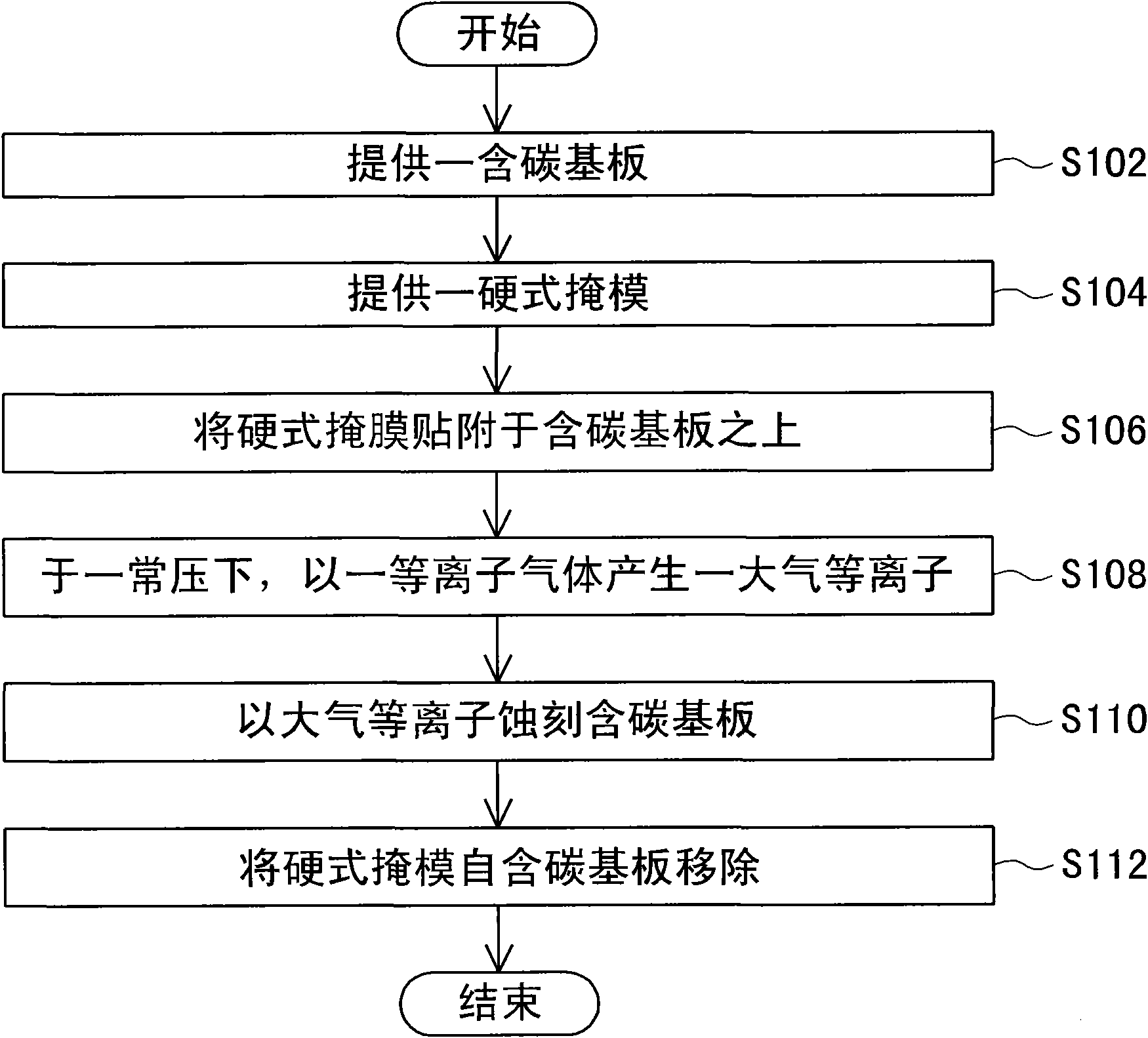
[0032] An embodiment is proposed below for detailed description, and the embodiment is only used as an example for illustration, and does not limit the scope of protection of the present invention. In addition, the drawings in the embodiments omit unnecessary components to clearly show the technical characteristics of the present invention.

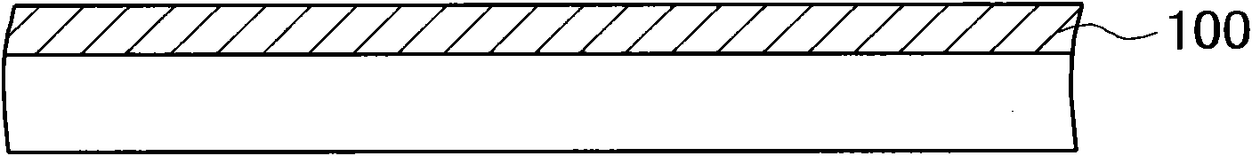
[0033] Please refer to figure 1 and Figure 2 to Figure 7 , figure 1 A flowchart illustrating a method for patterning a carbon-containing substrate 100, Figure 2 to Figure 7 draw figure 1 A schematic diagram of the steps.

[0034] First, in step S102, if figure 2 As shown, a carbon-containing substrate 100 is provided. In this embodiment, the carbon-containing substrate 100 is illustrated by taking a transparent carbon nanotube-based thin film (Transparent Carbon Nanotube-based Thin Film) as an example. The optical properties of the carbon nanotube transparent conductive film are similar to those of the indium tin oxide film (Ind...


PUM


Abstract

A patterning method for a carbon-based substrate is provided. The patterning method for the carbon-based substrate includes the following steps. The carbon-based substrate is provided. An atmospheric pressure plasma is produced from a plasma gas under an open air environment. The plasma gas includes oxygen. The carbon-based substrate is etched by the atmospheric pressure plasma. The invention is directed to the patterning method for the carbon-based substrate. The carbon-based substrate is etched by the oxygen-contained plasma at the atmospheric pressure, so that the process of patterning the carbon-based substrate is more efficient and more convenient.

Description

technical field [0001] The invention relates to a method for patterning a substrate, and in particular to a method for patterning a carbon-containing substrate. Background technique [0002] Due to the characteristics of high conductivity, high strength and flexibility, carbon-containing substrates have gradually attracted attention in recent years. If circuit patterns such as transistors are drawn on the carbon-containing substrate to make a transparent carbon nanotube-based thin film (Transparent Carbon Nanotube-based Thin Film), it can even have a multi-touch effect. In the case that the carbon nanotube transparent conductive film can reach 85% light transmittance and 200Ω / sq, it can already be applied to touch panels of various electronic products. [0003] Traditional semiconductor processes use lithography, wet etching and other processes to form circuits. However, the corrosion resistance of the carbon-containing substrate is quite good, making the patterning proces...

Claims


Application Information

Patent Timeline
Patent Type & Authority Applications(China)
IPC IPC(8): H01L21/768
CPCC23F1/00G06F3/045B82Y30/00
Inventor 张加强吴清吉黄淑娟许文通胡志明郭信良
Owner IND TECH RES INST
Why Eureka
Try Eureka