Integrated circuit structure

A technology of integrated circuits and gate electrodes, which is applied in the structure and formation of fin field effect transistors, can solve the problems of high substrate leakage current, achieve the effects of reducing junction area, optimizing work function, and increasing driving current

Active Publication Date: 2011-04-27
TAIWAN SEMICON MFG CO LTD
View PDF3 Cites 46 Cited by
  • Summary
  • Abstract
  • Description
  • Claims
  • Application Information

AI Technical Summary

Problems solved by technology

As a result, the substrate leakage current of

Method used


Image

  • Integrated circuit structure
  • Integrated circuit structure
  • Integrated circuit structure

Examples


Embodiment Construction

[0037] Embodiments of the present invention are enumerated below and described in detail with accompanying drawings. The elements and designs of the following embodiments are for the purpose of simplifying the disclosed inventions, but are not intended to limit the present invention.

[0038] The present invention proposes a novel embodiment of a fin field effect transistor and its method of formation, and describes the intermediate fabrication steps in the manufacture of this embodiment, and also discusses various variations of the embodiment shown in the embodiment and drawings, similar components are identified using similar reference numerals.

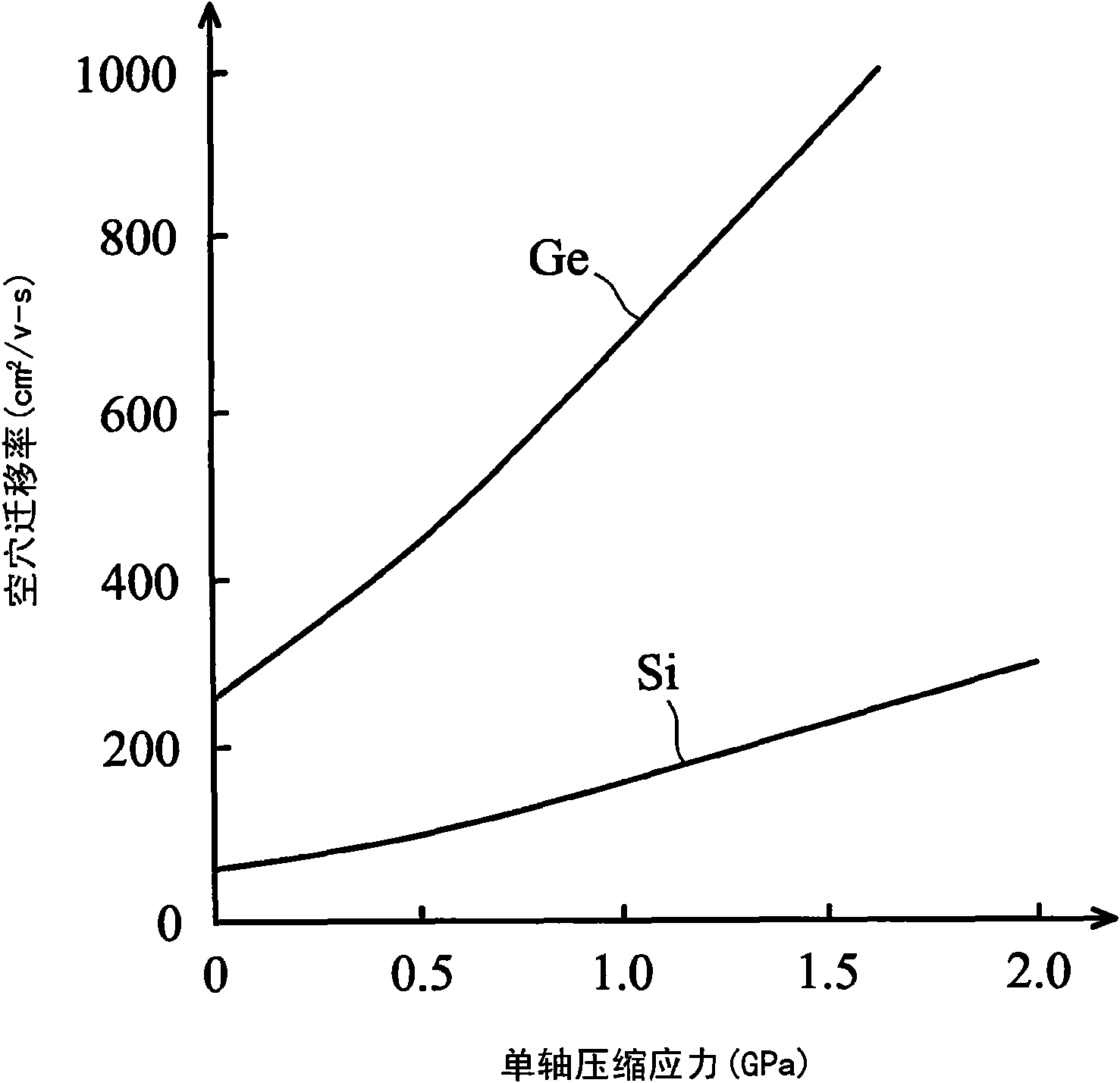
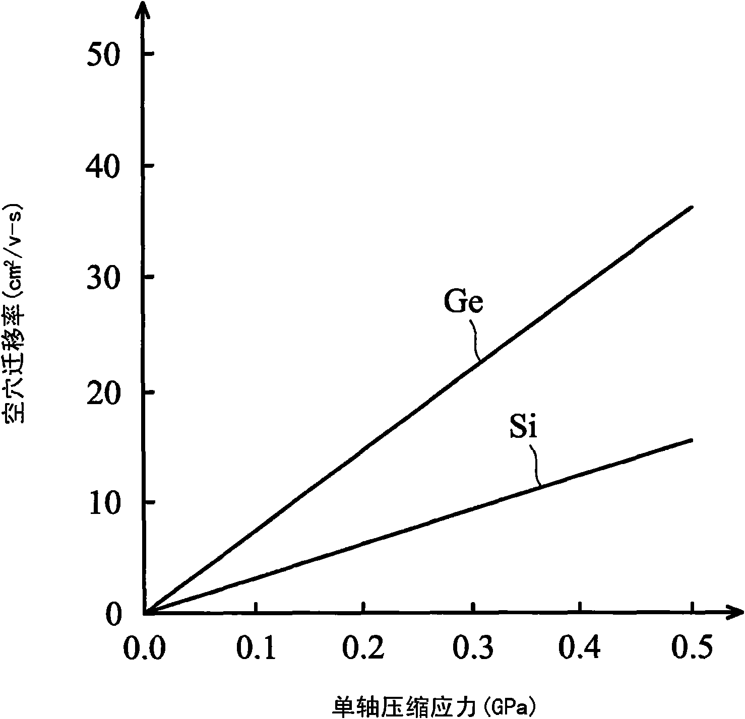
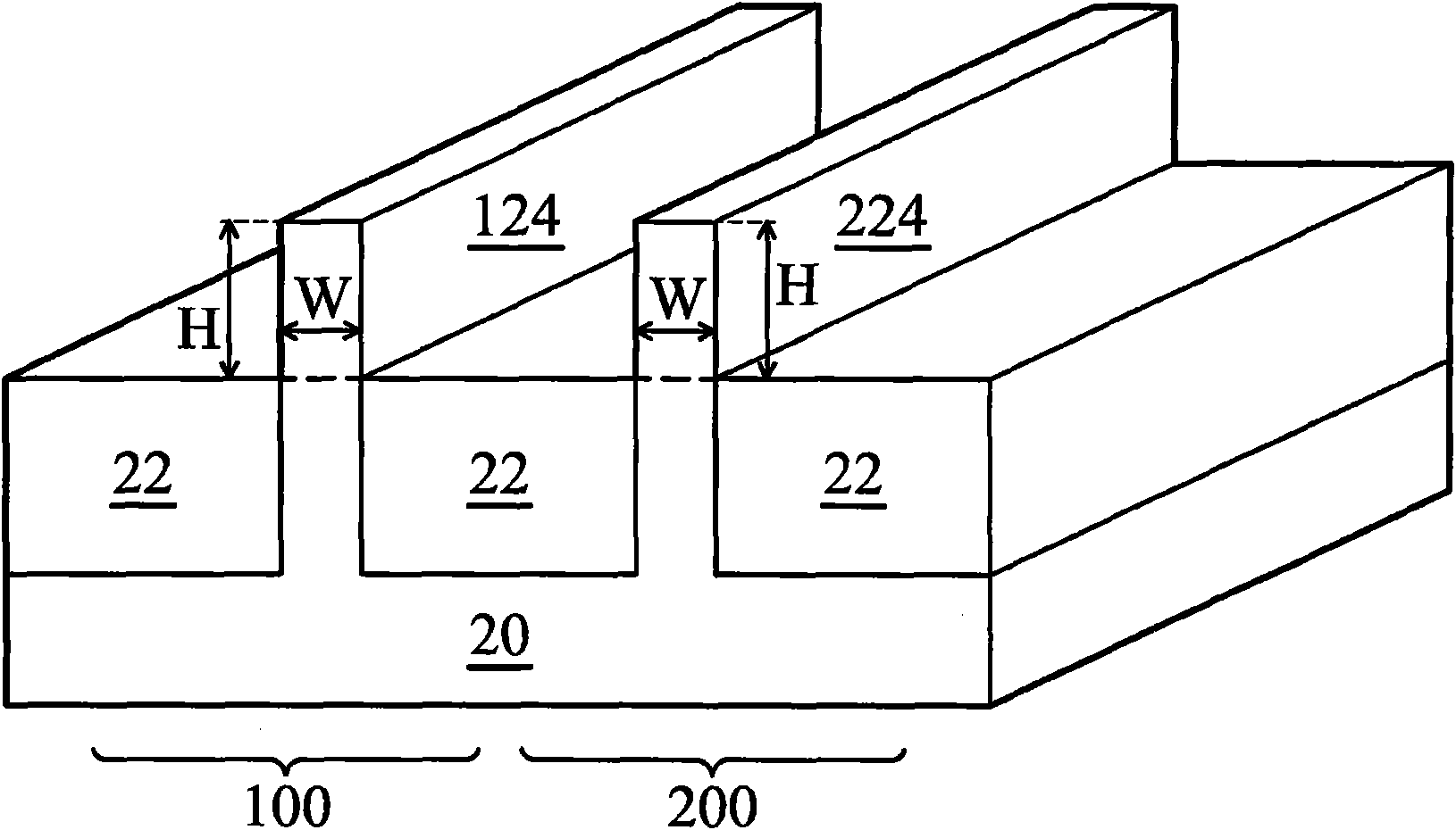
[0039] See image 3, forming an integrated circuit. The integrated circuit structure includes a substrate 20, which may be a silicon substrate, a germanium substrate, or a substrate formed of other semiconductor materials. The substrate 20 can be doped with p-type or n-type impurities. Isolation regions, such as shallow trench ...


PUM

PropertyMeasurementUnit
Work functionaaaaaaaaaa

Abstract

The invention provides an integrated circuit structure having an n-type fin field effect transistor (FinFET) and a p-type FinFET. The n-type FinFET includes a first germanium fin over a substrate; a first gate dielectric on a top surface and sidewalls of the first germanium fin; and a first gate electrode on the first gate dielectric. The p-type FinFET includes a second germanium fin over the substrate; a second gate dielectric on a top surface and sidewalls of the second germanium fin; and a second gate electrode on the second gate dielectric. The first gate electrode and the second gate electrode are formed of the same material having a work function close to an intrinsic energy level of germanium. The invention can simultaneously reach the requirements for optimizing the work functionsof n-type FinFETs and p-type FinFETs.

Description

technical field [0001] The present invention relates to an integrated circuit structure, and in particular to a fin field effect transistor (Finfield effect transistor, FinFET) structure and its forming method. Background technique [0002] The speed of metal-oxide-semiconductor (MOS) transistors is closely related to the drive current of the MOS, and the drive current is closely related to the mobility of charges. For example, an n-type metal-oxide-semiconductor (NMOS) transistor has a larger drive current when electrons have higher electron mobility in its channel, and when holes have higher hole mobility in its channel , the p-type metal oxide semiconductor (PMOS) transistor has a larger drive current. [0003] Germanium (Ge) is a known semiconductor material. Germanium has higher electron and hole mobility than silicon (2.6 times and 4 times, respectively), and germanium is a semiconductor material commonly used to form integrated circuits. Therefore, germanium is an ...

Claims


Application Information

Patent Timeline
IPC IPC(8): H01L29/78H01L29/43
CPCH01L21/823814H01L29/6681H01L21/823821H01L21/823807H01L29/7848H01L29/66795H01L29/785H01L21/02532H01L21/02535H01L21/76224H01L21/823878H01L21/8256H01L29/0847
Inventor 叶致锴张智胜万幸仁
Owner TAIWAN SEMICON MFG CO LTD
Why Eureka
Try Eureka