
Method for forming fuse structure

A technology of fuse structure and polysilicon fuse, which is applied in the field of semiconductor technology, can solve the problems of damage to internal circuits, the total thickness of the dielectric layer, and the inability to accurately control the thickness, and achieve the effect of avoiding damage

Inactive Publication Date: 2011-05-11
CSMC TECH FAB1 +1
View PDF0 Cites 4 Cited by
  • Summary
  • Abstract
  • Description
  • Claims
  • Application Information

AI Technical Summary

Problems solved by technology

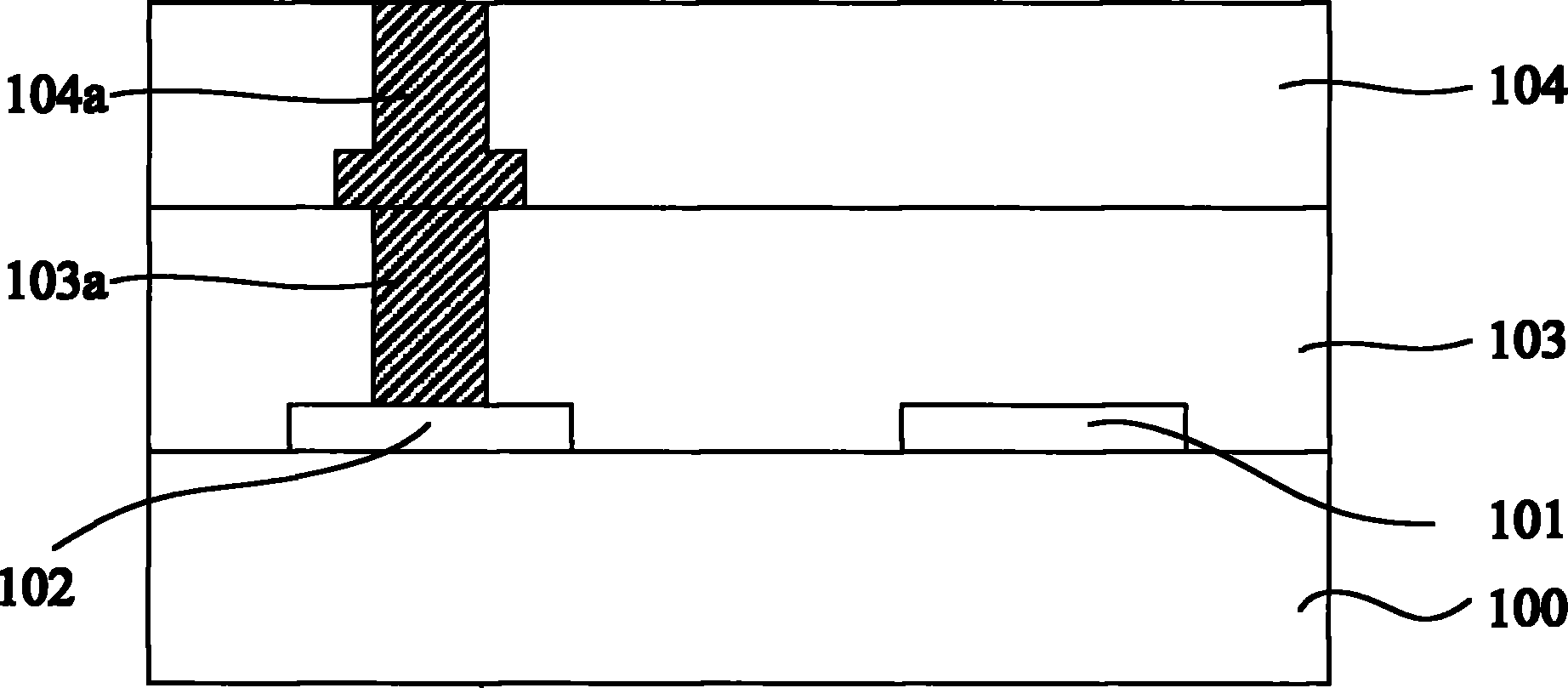
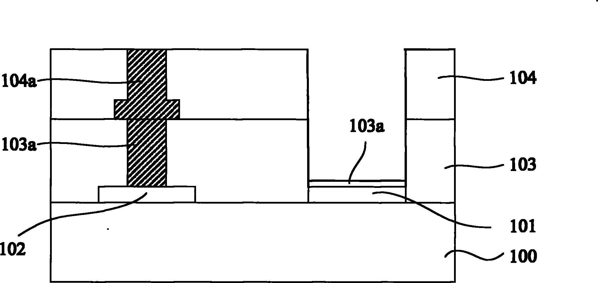
However, in the prior art, the thickness of the remaining first dielectric layer 103a cannot be accurately controlled during the etching process. If the etching amount is too large, the fuse structure 101 will be damaged; The thickness of the remaining first dielectric layer 103a is too large. When the fuse structure 101 is blown, the generated product cannot burst the remaining first dielectric layer 103a, so that the product cannot be discharged upward, resulting in lateral Swell and damage the internal circuitry
Moreover, as the technology level and circuit complexity increase, the number of layers of the metal interconnection structure gradually increases, so the total thickness of the dielectric layers accumulated on the fuse structure 101 becomes very large, making the etching process more precise. hard to control

Method used


Image

  • Method for forming fuse structure
  • Method for forming fuse structure
  • Method for forming fuse structure

Examples


Embodiment Construction

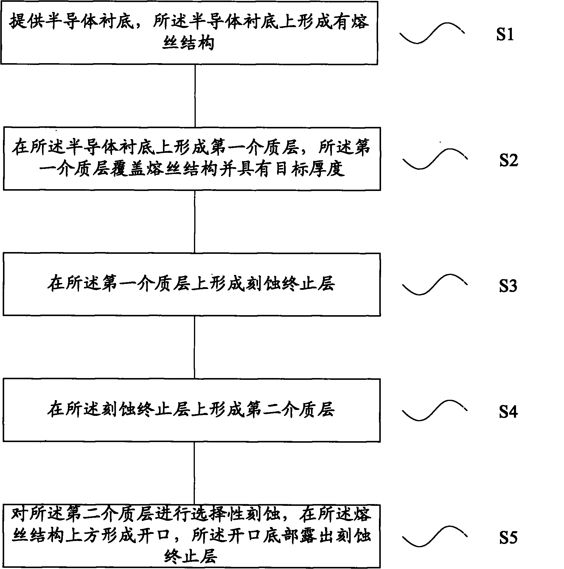
[0030] In the formation process of the fuse structure, in order to improve the reliability of the device, it is necessary to effectively control the thickness of the dielectric layer remaining above the fuse structure. The present invention forms a first dielectric layer with a target thickness above the fuse structure, and An etch stop layer is formed on the first dielectric layer, so that the etching process during the opening formation process stops automatically at the etch stop layer, thereby effectively controlling the thickness of the remaining dielectric layer above the fuse structure and preventing the fuse structure from being blown. Lateral expansion can cause damage to the circuit.

[0031] In order to make the above objects, features and advantages of the present invention more comprehensible, specific implementations of the present invention will be described in detail below in conjunction with the accompanying drawings.

[0032] In the following description, spe...


PUM


Abstract

The invention relates to a method for forming a fuse structure which comprises the following steps: providing a semiconductor substrate, forming a fuse structure on the semiconductor substrate; forming a first dielectric layer with a target thickness on the semiconductor substrate for covering the fuse structure; forming an etching termination layer on the first dielectric layer; forming a second dielectric layer on the etching termination layer; selectively etching the second dielectric layer; and forming an opening above the fuse structure, and exposing the bottom of the opening out of the etching termination layer. The method provided by the invention can efficiently control the thickness of the dielectric layer resided above the fuse structure and increase the reliability of elements.

Description

technical field [0001] The invention relates to the field of semiconductor technology, in particular to a method for forming a fuse structure. Background technique [0002] With the improvement of the semiconductor process level and the increase of the complexity of the integrated circuit, the semiconductor components become more susceptible to various defects, and the failure of a single component such as a transistor or a memory unit often leads to the failure of the entire integrated circuit. defect. A common solution is to form some fusible connection lines in the integrated circuit, that is, fuse structures, so as to ensure the availability of the integrated circuit. [0003] Generally speaking, the fuse structure is used to connect redundant circuits in an integrated circuit. When a defect occurs in the circuit, the fuse is blown, and the redundant circuit is used to repair or replace the defective circuit. The fuse structure is often used in memory. When the product...

Claims


Application Information

Patent Timeline
IPC IPC(8): H01L21/768
CPCH01L21/31116H01L23/62H01L2924/0002
Inventor 匡金祝孔维张明敏赵志勇
Owner CSMC TECH FAB1
Learn More