Method and equipment for processing PCB (Printed Circuit Board)

A PCB board and processing method technology, applied in the field of printed circuit board processing, can solve the problems of poor drilling hole position accuracy, poor positioning accuracy, low processing efficiency, etc., to achieve convenient machining, reduce burrs and drilling pollution, improve The effect of processing efficiency

Active Publication Date: 2011-05-11
SHENNAN CIRCUITS
View PDF4 Cites 5 Cited by
  • Summary
  • Abstract
  • Description
  • Claims
  • Application Information

AI Technical Summary

Problems solved by technology

[0006] 1) The temperature in the machining workshop is generally 21+ / -2°C, and the PCB board taken out of the refrigerator will quickly return to the greenhouse after processing, requiring multiple cooling times, and the processing efficiency is low;
[0007] 2) It needs multiple disassembly and assembly, and the positioning accuracy is poor, which makes the machining accuracy worse, such as the hole position accuracy of the drilling hole;
[0008] 3) Frequent cooling operations make it easy to generate water vapor on the surface of the plate, and the adsorption of dust makes processing debris more difficult to remove

Method used


Image

  • Method and equipment for processing PCB (Printed Circuit Board)
  • Method and equipment for processing PCB (Printed Circuit Board)
  • Method and equipment for processing PCB (Printed Circuit Board)

Examples


Embodiment Construction

[0028] In order to describe in detail the technical content, structural features, achieved objectives and effects of the present invention, the following is a detailed description in conjunction with the embodiments and accompanying drawings.

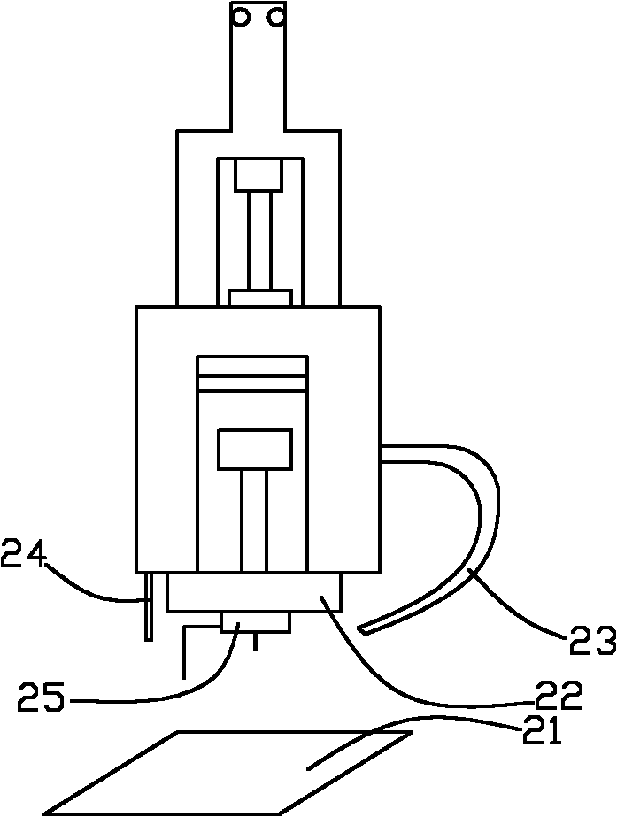
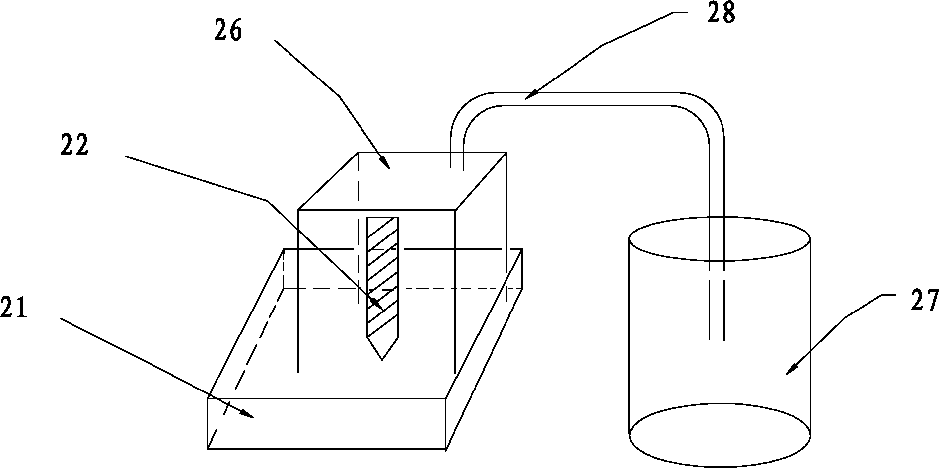
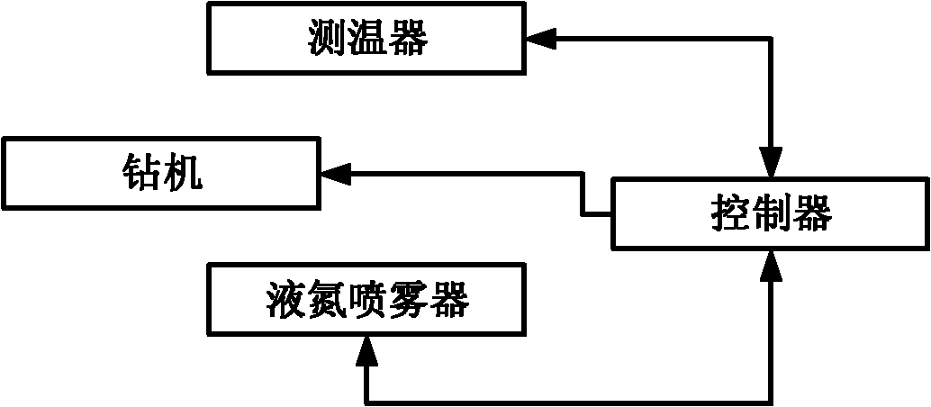
[0029] As an embodiment of the PCB board processing method of the present invention, during the mechanical processing of the PCB board, the temperature of the PCB board to be processed is always controlled below the glass transition temperature by using a cooling liquid or a cooling solid. Taking the PCB material as PTFE material as an example, the temperature of the PCB board to be processed is always controlled below 25°C.

[0030] The PCB board processing method of the present invention uses coolant or cooling solid to directly cool the PCB board to be processed at the processing site, and the temperature of the PCB board to be processed is always controlled below the glass transition temperature. Hard and brittle, convenient for mechanic...


PUM


Abstract

The invention belongs to the technical field of PCB (printed circuit board) processing, and especially relates to a method and equipment for processing a PCB. The processing method provided by the invention comprises the following step: controlling the temperature of the part to be processed of the PCB below the glass-transition temperature by utilizing a cooling liquid or a cooling solid in the course of mechanically processing the PCB. The processing method of the PCB provided by the invention directly cools the part to be processed of the PCB by utilizing the cooling fluid or the cooling solid in the processing site and controls the temperature of the part to be processed of the PCB below the glass-transition temperature, at the moment, the material is relatively hard and brittle, thereby being convenient for the mechanical processing and being capable of reducing the burr and drilling dirt on the PCB. Because the on-site processing is adopted, the invention can guarantee the cooling requirement and simultaneously omit the operations of repeatedly disassembling, assembling and positioning PCB pieces and then freezing by putting pieces into a refrigerator, thereby greatly enhancing the processing efficiency. Because the PCB pieces do not need to be repeatedly disassembled and assembled, the accuracy of a processing region cannot be influenced by the positioning for multiple times.

Description

Technical field [0001] The invention belongs to the technical field of printed circuit board (PCB board) processing, and particularly relates to a method and equipment for processing a PCB board. Background technique [0002] In the PCB manufacturing process, mechanical processing of the sheet is required, such as drilling, trimming, hollowing, etc., but the glass transition temperature of some materials is very low, and the high temperature generated during mechanical processing can easily exceed the glass of this material Transition temperature. When the processed material is at or above the glass transition temperature of the material, the material will become soft and not easy to cut. The processed debris is entangled on the surface of the processing tool, resulting in poor chip removal and easy on the PCB. Produce a lot of burrs and drilling dirt. [0003] For example, when the processing material is polytetrafluoroethylene (Polytetrafluoroethylene ptfe, abbreviated as PTFE) ...

Claims


Application Information

Patent Timeline
Patent Type & Authority Applications(China)
IPC IPC(8): H05K3/00
CPCH05K3/0047
Inventor 缪桦龚小林王成勇彭勤卫
Owner SHENNAN CIRCUITS
Why Eureka
Try Eureka